Ordered germanium nanowires on silicon substrate and its preparation method and application

A germanium nanowire and silicon substrate technology, applied in the field of materials, can solve the problems of incompatibility, complex germanium nanowire-assisted transfer and arrangement technology, affecting device performance, etc.

Active Publication Date: 2021-04-27
INST OF PHYSICS - CHINESE ACAD OF SCI
View PDF9 Cites 0 Cited by
  • Summary
  • Abstract
  • Description
  • Claims
  • Application Information

AI Technical Summary

Problems solved by technology

[0006] 1. There is metal contamination in germanium nanowires obtained by the commonly used gas-liquid-solid method, which affects device performance;
[0007] 2. Germanium nanowires are non-in-plane growth, which is not compatible with the current process;
[0008] 3. Germanium nanowire assisted transfer arrangement technology is complicated, low in efficiency, and difficult to achieve high-density orderly arrangement;
[0009] 4. The mixture of light and heavy holes in germanium nanowires is not conducive to the improvement of qubit decoherence time

Method used


Image

  • Ordered germanium nanowires on silicon substrate and its preparation method and application
  • Ordered germanium nanowires on silicon substrate and its preparation method and application
  • Ordered germanium nanowires on silicon substrate and its preparation method and application

Examples


Embodiment 1

[0047] This example is used to illustrate the ordered germanium nanowires and the preparation method thereof of the present invention.

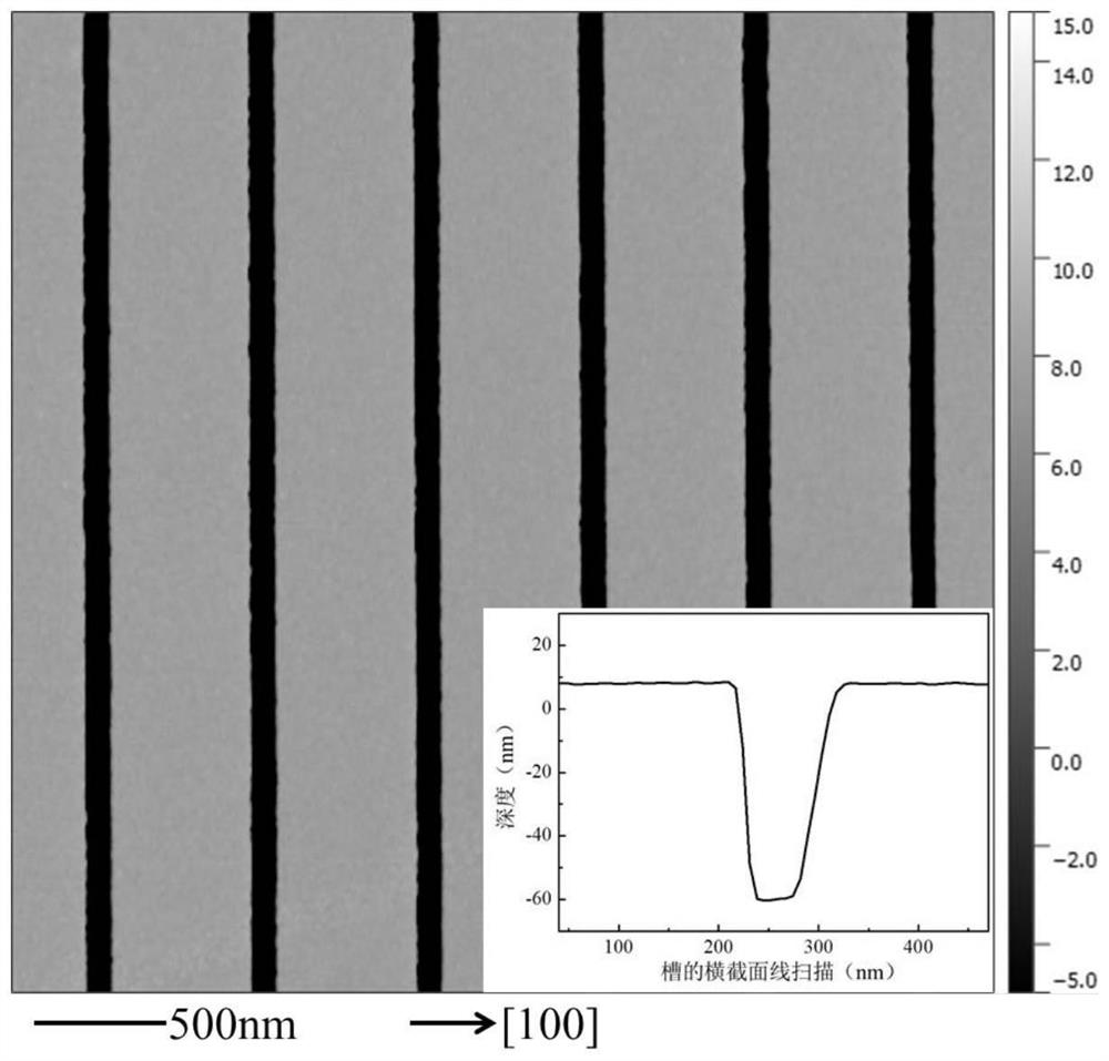
[0048] (1) Obtain a periodic groove structure on a silicon (001) substrate:

[0049] Spin-coat resist (PMMA) on the surface of silicon (001) substrate; use electron beam exposure technology to form a periodic groove structure along the [100] or [010] direction on the resist; use inductively coupled plasma The periodic groove structure is transferred to the silicon (001) substrate by bulk reactive ion etching technology; the residual resist on the substrate surface is removed by oxygen plasma.

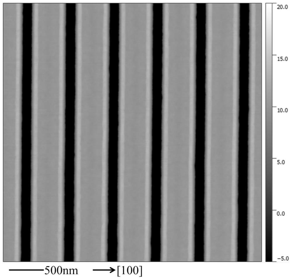
[0050] (2) Using molecular beam epitaxy growth technology to epitaxially grow a 3nm silicon germanium layer on a silicon (001) substrate with a periodic groove structure, the content of germanium is 25%, and the growth temperature is 550 ° C. On the edge of each groove An ordered trapezoidal linear structure is formed.

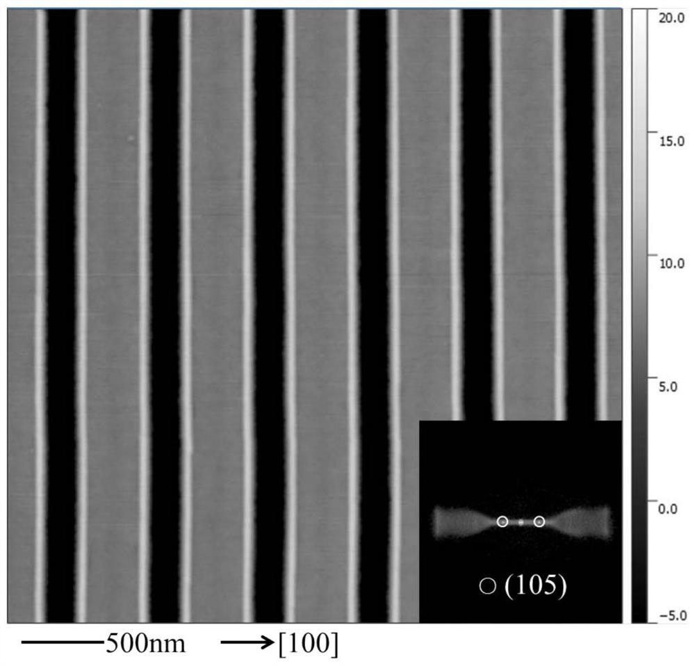
[0051] (3) A 0.6nm pure germani...

Embodiment 2

[0059] This example is used to illustrate the ordered germanium nanowires and the preparation method thereof of the present invention.

[0060] (1) Obtain a periodic groove structure on a silicon (001) substrate:

[0061] Spin-coat resist (PMMA) on the surface of silicon (001) substrate; use electron beam exposure technology to form a periodic groove structure along the [100] or [010] direction on the resist; use inductively coupled plasma The periodic groove structure is transferred to the silicon (001) substrate by bulk reactive ion etching technology; the residual resist on the substrate surface is removed by oxygen plasma.

[0062] (2) Using molecular beam epitaxy growth technology to epitaxially grow a 5nm silicon germanium layer on a silicon (001) substrate with a periodic groove structure, the content of germanium is 20%, and the growth temperature is 540 ° C. On the edge of each groove An ordered trapezoidal linear structure is formed.

[0063] (3) Using molecular be...


PUM

PropertyMeasurementUnit
thicknessaaaaaaaaaa
depthaaaaaaaaaa
depthaaaaaaaaaa

Abstract

The invention provides an ordered germanium nanowire on a silicon substrate, comprising a silicon substrate with a periodic groove structure and a platform structure on the surface, a silicon germanium layer on the silicon substrate, and a silicon germanium layer on the silicon germanium layer. layer of pure germanium. The present invention also provides a method for preparing the ordered germanium nanowire on the silicon substrate of the present invention, comprising the following steps: (1) obtaining an ordered periodic groove structure and platform structure on the silicon substrate; (2) Epitaxial growth of a silicon germanium layer on the surface of a silicon substrate with a periodic groove structure and a platform structure; (3) epitaxial growth of a pure germanium layer on the surface of the silicon germanium layer, and then performing in-situ annealing on the material. The invention also provides the application of the ordered germanium nanowires on the silicon substrate of the invention in hole spin qubits and integrated devices thereof. The ordered germanium nanowires on the silicon substrate provided by the invention have high hole mobility and are helpful for the separation of heavy holes and light holes, thereby being beneficial to the improvement of qubit decoherence time.

Description

technical field [0001] The present invention belongs to the field of materials. Specifically, the present invention relates to an ordered germanium nanowire on a silicon substrate, its preparation method and application. Background technique [0002] The rapid development of the information age has made classical computers unable to meet the huge data computing and processing needs, while quantum computing is considered to be an effective way to greatly improve data computing and processing. Huge sums of money have been invested in the research of quantum computing. The basic unit of quantum computing is the qubit, and the spin qubit based on semiconductor nanowire quantum dots has attracted extensive attention because of its great advantages in information reading, scalability and integration. Among them, the preparation of ordered nanowires is an important basis for the realization of qubits and their integration technology research. [0003] Group IV semiconductor nano...

Claims


Application Information

Patent Timeline
Patent Type & Authority Patents(China)
IPC IPC(8): H01L21/02H01L29/06B82Y40/00
CPCB82Y40/00H01L21/02381H01L21/0243H01L21/02532H01L21/02603H01L21/0262H01L29/0673
Inventor 张建军高飞
Owner INST OF PHYSICS - CHINESE ACAD OF SCI
Why Eureka
Try Eureka