Semiconductor product insulation layer structure and preparation method thereof

A technology of semiconductor and insulating layer, applied in semiconductor/solid-state device manufacturing, semiconductor device, semiconductor/solid-state device components, etc., can solve the problem of difficult to achieve better radio frequency performance, poor thermal conductivity of insulating layer, poor circuit performance, etc. problem, to achieve the effect of reducing nucleation energy, high dielectric constant, and good insulation

Inactive Publication Date: 2019-08-02
SHENYANG SILICON TECH
View PDF9 Cites 8 Cited by
  • Summary
  • Abstract
  • Description
  • Claims
  • Application Information

AI Technical Summary

Problems solved by technology

One of the main problems is the self-heating effect, which is caused by the insulating layer SiO 2 Poor thermal conductivity (its thermal conductivity is only nearly 1% of that of silicon) causes overheating failure of devices;
[

Method used


Image

  • Semiconductor product insulation layer structure and preparation method thereof
  • Semiconductor product insulation layer structure and preparation method thereof
  • Semiconductor product insulation layer structure and preparation method thereof

Examples


Embodiment 1

[0072] An insulating layer structure for a semiconductor product, which is composed as follows: a device substrate 1, a supporting substrate 2, and a film layer 3; wherein: the device substrate 1 and the supporting substrate 2 are both silicon wafers; Arranged on the substrate 1 and / or the supporting substrate 2; the thin film layer 3 is one of the following: a silicon dioxide layer, a silicon oxynitride layer, a silicon nitride layer, a polysilicon layer and an amorphous silicon layer;

[0073] One of the device substrate 1 and / or the supporting substrate 2 and the other are bonded together through at least one thin film layer 3 arranged on one of them to form a whole to form a multilayer SOI structure (that is: on an insulating substrate silicon structure).

[0074] The insulating layer structure for the semiconductor product satisfies the combination of the following requirements:

[0075] First, the resistivity of the silicon wafer used as the device substrate 1 or / and su...

Embodiment 2

[0123] The content of this embodiment is basically the same as that of Embodiment 1, the difference is that:

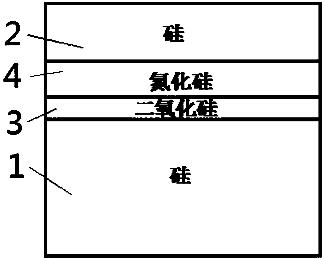
[0124] Insulating layer structures for semiconductor products such as figure 1 Said, the composition of insulating layer structure for semiconductor products is as follows: device substrate 1, supporting substrate 2, thin film layer 3; Wherein: both of device substrate 1, supporting substrate 2 are silicon wafers; Arranged on the substrate 1 and / or the supporting substrate 2; the film layer 3 is a silicon dioxide layer;

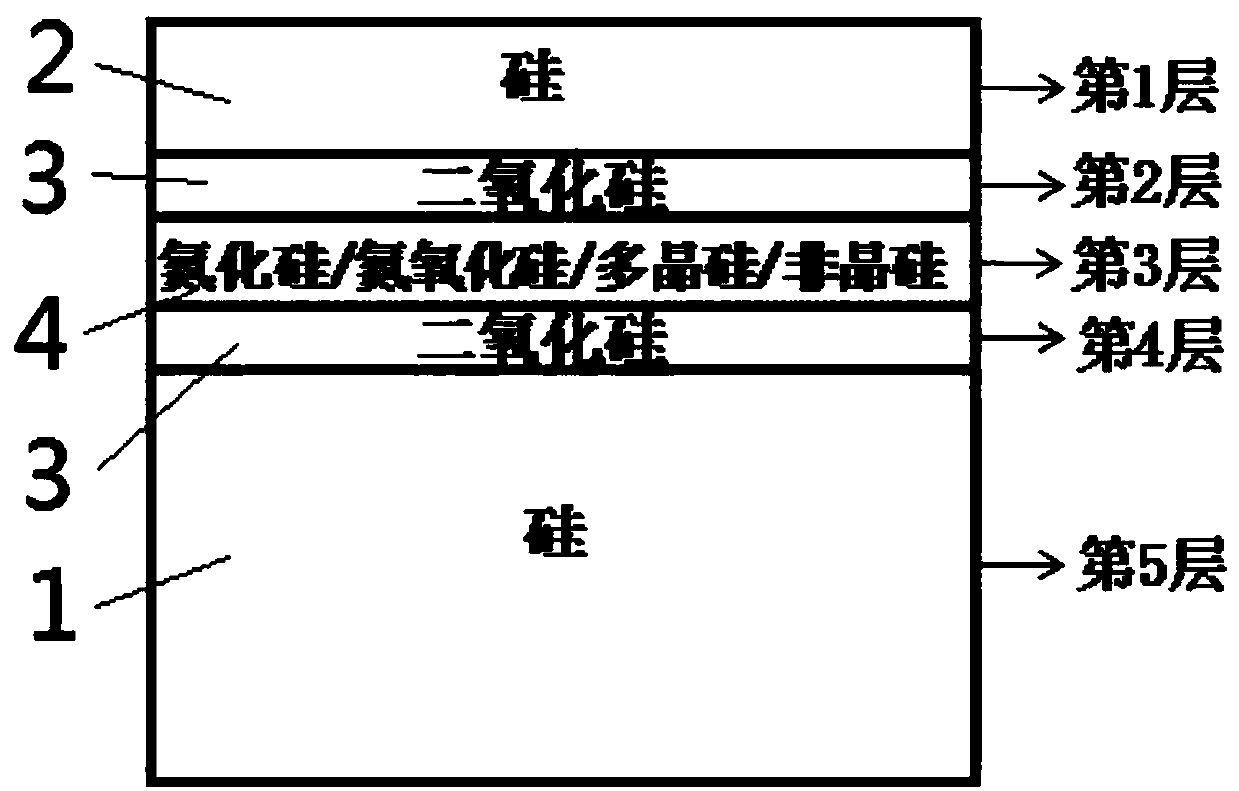
[0125] At least one intermediate layer 4 is arranged on the film layer 3 of at least one of the device substrate 1 and the supporting substrate 2, and the intermediate layer 4 is one of the following: silicon nitride oxide layer, silicon nitride layer , a polysilicon layer and an amorphous silicon layer;

[0126] An intermediate layer 4 is arranged on at least one of the film layer 3 of the device substrate 1 and / or the support substrate 2; both th...

Embodiment 3

[0128] The content of this embodiment is basically the same as that of Embodiment 1, the difference is that:

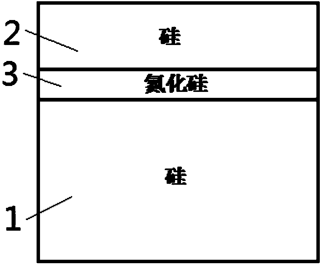
[0129] Insulating layer structures for semiconductor products such as figure 2 Said, the composition of insulating layer structure for semiconductor products is as follows: device substrate 1, supporting substrate 2, thin film layer 3; Wherein: both of device substrate 1, supporting substrate 2 are silicon wafers; Arranged on the substrate 1 and / or the supporting substrate 2; the film layer 3 is a silicon nitride layer; one of the device substrate 1 and / or the supporting substrate 2 and the other pass at least one of the thin films arranged on one of them The layers 3 are bonded together to form a whole to form a multilayer SOI structure (ie: a silicon-on-insulator structure).


PUM

PropertyMeasurementUnit
Thicknessaaaaaaaaaa
Single layer thicknessaaaaaaaaaa
Diameteraaaaaaaaaa

Abstract

The invention relates to a semiconductor product insulation layer structure. Both a device substrate (1) and a support substrate (2) are silicon wafers, a film layer (3) is arranged on the device substrate (1) and/or the support substrate (2), the film layer (3) is one of materials as follows, a silicon dioxide layer, a silicon oxynitride layer, a silicon nitride layer, a polysilicon layer and anamorphous silicon layer, and one of the device substrate (1) and/or the support substrate (2) and the other are bonded together through the film layer (3) disposed on at least one of the two to form an integrally multi-layer SOI structure. The invention further relates to a preparation method of the semiconductor product insulation layer structure. The special insulation layer structure is diverse, problems of serious self-heating, serious SOI warpage change caused by high-temperature annealing and poor radio frequency characteristics of an SOI device in the prior art are solved, and relatively expected large economic and social values can be achieved.

Description

[0001] Technical field: [0002] The invention relates to the technical field of semiconductor material preparation, and in particular provides an insulating layer structure for semiconductor products formed by a bonding process and a preparation method thereof. [0003] Background technique: [0004] In the prior art, due to the unique advantages of the SOI (Silicon On Insulator, silicon on insulating layer) structure, devices based on this structure will substantially reduce junction capacitance and leakage current, increase switching speed, reduce power consumption, and realize High-speed, low-power operation, its performance is significantly better than bulk silicon devices and circuits. At present, the application of SOI devices has gradually expanded from military, aerospace and industry to data processing, communication and consumer electronics and other fields. As a next-generation silicon-based integrated circuit technology, SOI technology is widely used in most field...

Claims


Application Information

Patent Timeline
IPC IPC(8): H01L21/762H01L27/12
CPCH01L21/76254H01L27/1203H01L21/022H01L21/02301H01L21/02334H01L21/0234H01L21/76251H01L21/02054H01L21/3226H01L23/585H01L23/66H01L29/0649
Inventor 高文琳李响柳清超
Owner SHENYANG SILICON TECH
Why Eureka
Try Eureka