A kind of suspended black dielectric thin film and its preparation method and application

A dielectric thin film and thin film technology are applied in the field of suspended black dielectric thin film and its preparation, which can solve the problems of low infrared absorption rate, large heat loss of two-dimensional thin film, and inability to prepare in batches, etc.

Active Publication Date: 2021-09-24
SHANGHAI INST OF MICROSYSTEM & INFORMATION TECH CHINESE ACAD OF SCI
View PDF0 Cites 0 Cited by
  • Summary
  • Abstract
  • Description
  • Claims
  • Application Information

AI Technical Summary

Problems solved by technology

[0004] The purpose of the present invention is to provide a suspended black dielectric thin film and its preparation method and application, thereby solving the problem of large heat loss and low infrared absorption rate of the two-dimensional thin film in the current MEMS sensor in the prior art, and the fact that the existing preparation method is not compatible with CMOS The process is compatible and cannot be prepared in batches

Method used


Image

  • A kind of suspended black dielectric thin film and its preparation method and application
  • A kind of suspended black dielectric thin film and its preparation method and application
  • A kind of suspended black dielectric thin film and its preparation method and application

Examples


Embodiment Construction

[0034] The present invention will be further described below with reference to the specific embodiments. It will be appreciated that the following examples are intended to illustrate the invention and are not intended to limit the scope of the invention.

[0035] According to a preferred embodiment of the present invention, there is provided a dielectric thin film method for preparing a black floating, the following steps:

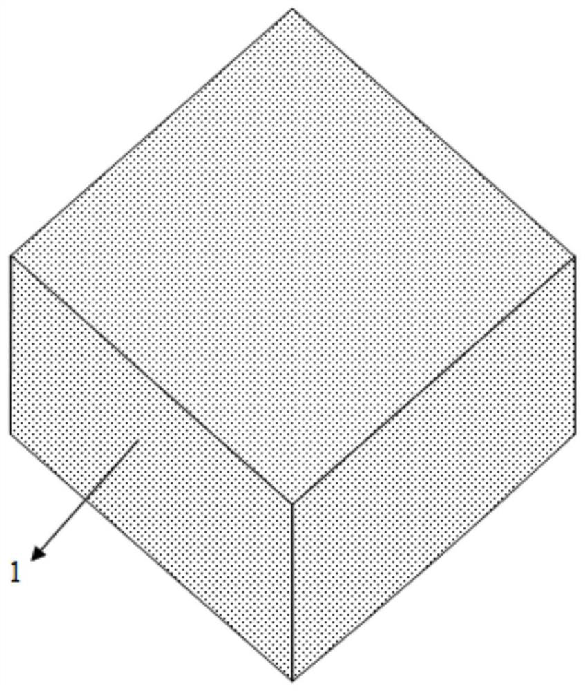
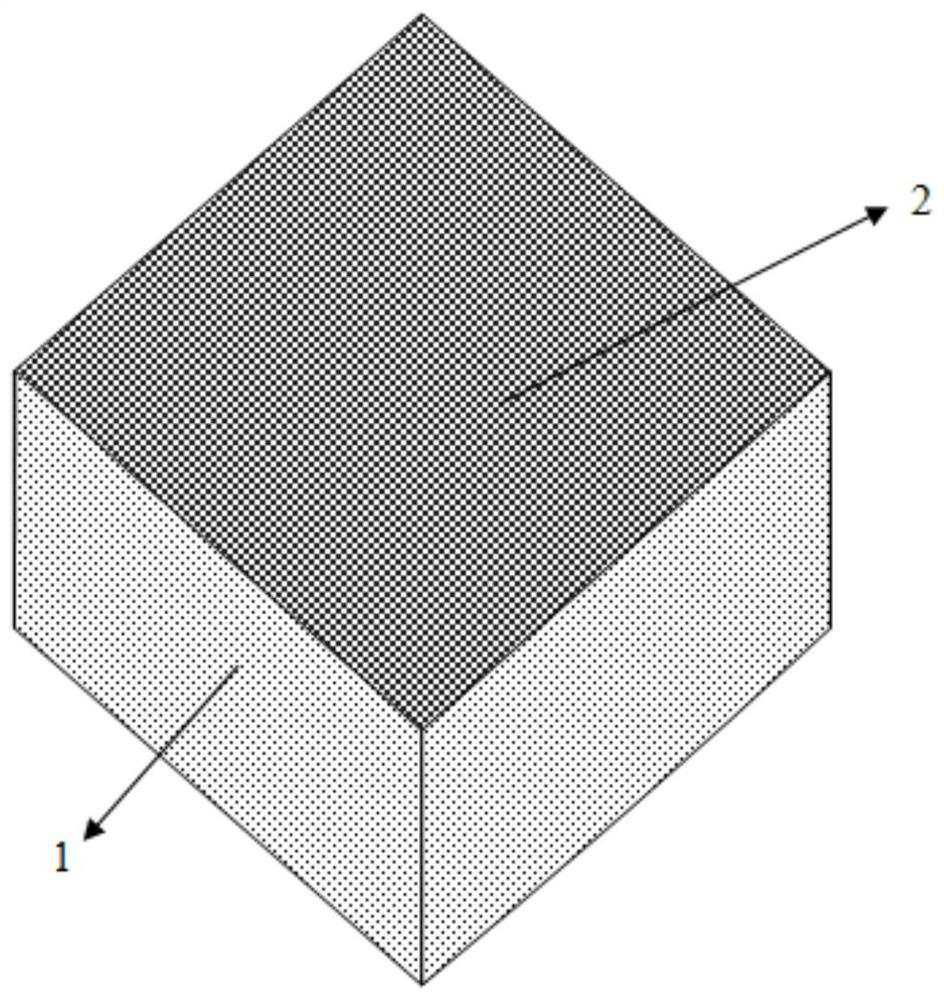
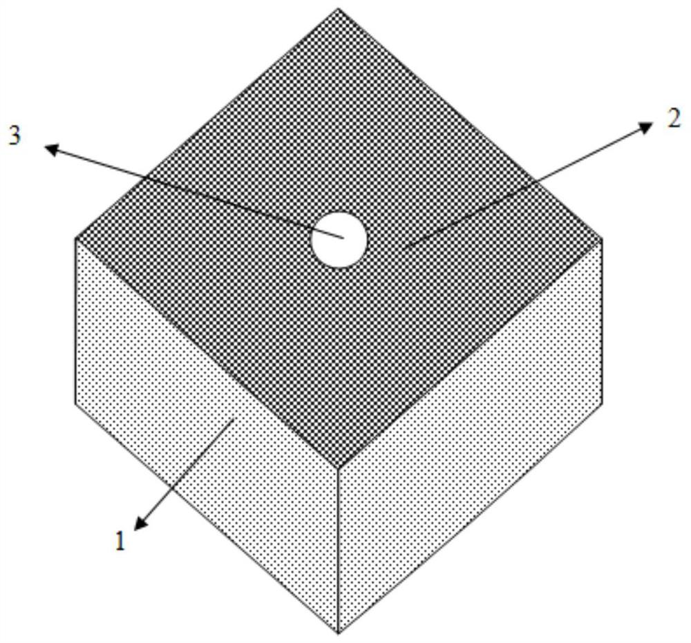
[0036]1) Select a (100) crystal face of the double-side polished single crystal silicon substrate 1, a wafer trimming large crystal orientation crystal orientation, the wafer size is 4 inches and a thickness of 400um ~ 420um, resistance of 3 to 8 ohm cm, doping type is N-type, such as figure 1 Indicated. In fact, the step of the semiconductor substrate 1) in the selected single crystal silicon substrate is not limited, and may be an SOI substrate or a germanium substrate and the like.

[0037] 2) using the standard cleaning process in a semiconductor process ...


PUM

PropertyMeasurementUnit
residual stressaaaaaaaaaa

Abstract

The present invention provides a suspended black dielectric film and its preparation method and application, including: S1: providing a semiconductor single crystal substrate, preparing a film mask on the surface of the substrate, and etching a window array to expose the window The surface of the semiconductor single crystal substrate in the array; S2: use wet technology to etch the surface of the semiconductor single crystal substrate to form a micro-nano pyramid structure; S3: remove the film mask, and then prepare on the surface of the semiconductor single crystal substrate film, preparing a black dielectric film on the surface of the micro-nano pyramid structure; S4: patterning the film and etching the film to form a release area; and S5: using dry etching technology or wet etching technology to release the black dielectric film and The supporting membrane structure is obtained. The present invention adopts micro-processing technology, and uses the micro-nano pyramid structure as a mold to prepare suspended black dielectric films in batches. The films can be widely used in the fields of light detection and light sources for enhancing light absorption radiation and reducing heat loss in the future.

Description

Technical field [0001] The present invention relates to a thin film manufacturing MEMS sensors, and more particularly, to a method for preparing a black and a dielectric thin film and apply a vacant. Background technique [0002] Art MEMS sensors, and the light absorption on the heat transfer problems are two important issues. In the field of gas sensors, the MEMS sensor is based on an organic or inorganic coating gas sensitive material is the mainstream of today's devices, but these materials require a temperature of at least 260 degrees C will have a strong response, in addition to the development of gas-sensitive material of the outer, how to reduce the thermal conductivity, reduce power consumption and improve thermal stability of such devices is the focus of research. In an infrared absorption art, such as infrared sensors, etc., since the two-dimensional planar material absorption efficiency of light is not very strong, how to enhance the light absorption rate and increase ...

Claims


Application Information

Patent Timeline
Patent Type & Authority Patents(China)
IPC IPC(8): B81C1/00B81B7/00
CPCB81B7/0083B81C1/00444B81C1/00476B81C1/00523B81C1/0069
Inventor 李铁何云乾刘延祥王跃林
Owner SHANGHAI INST OF MICROSYSTEM & INFORMATION TECH CHINESE ACAD OF SCI
Why Eureka
Try Eureka