Method for preparing elastic circuit board and elastic circuit board
A circuit board and elastic technology, applied in the manufacture of printed circuits, removal of conductive materials by chemical/electrolytic methods, printed circuits, etc., can solve problems such as poor tensile properties of elastic circuit boards, and achieve overcoming difficulties in welding and excellent ductility. , the effect of excellent mechanical and electrical properties
- Summary
- Abstract
- Description
- Claims
- Application Information
AI Technical Summary
Problems solved by technology
Method used
Image
Examples
preparation example Construction
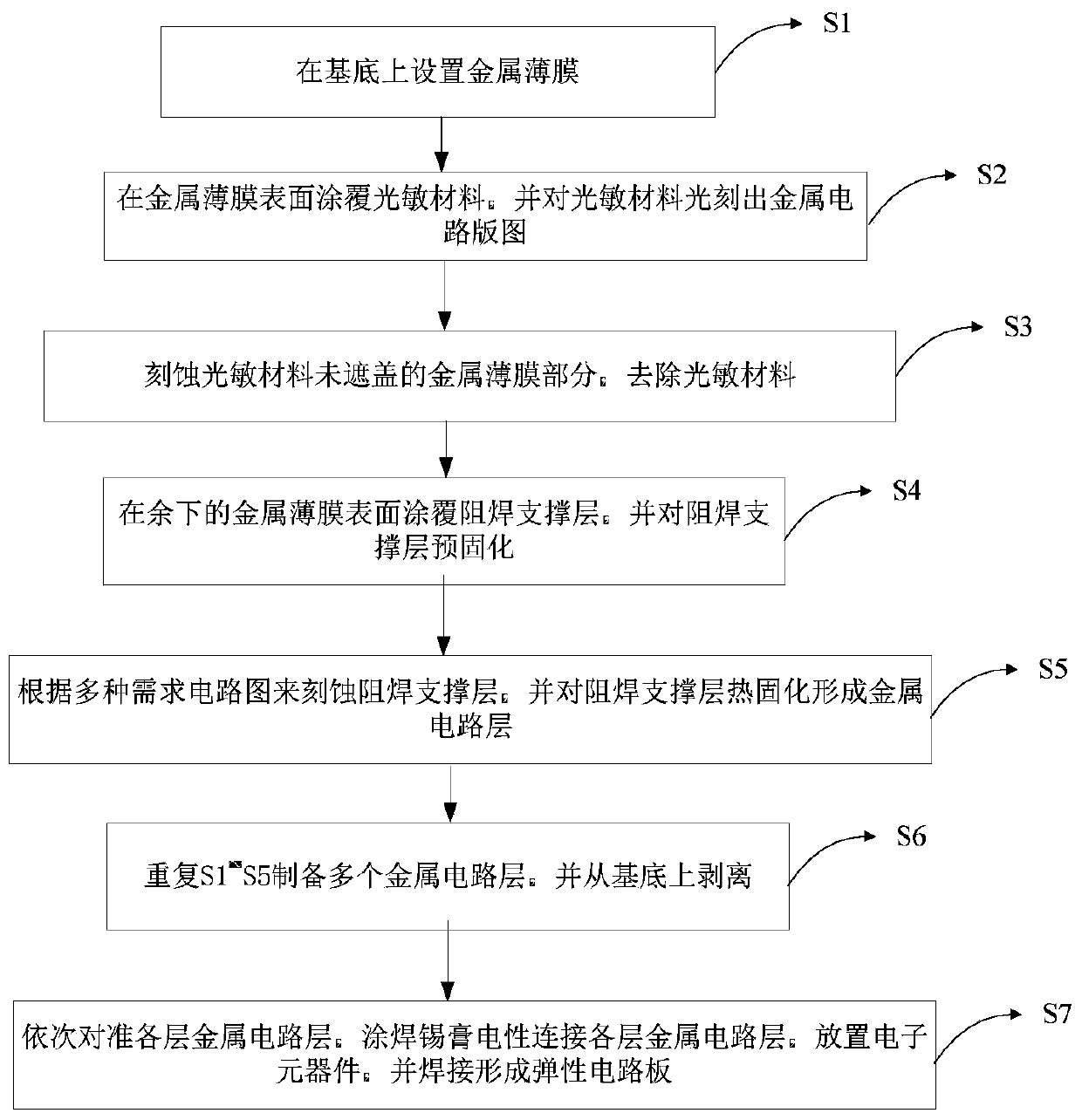
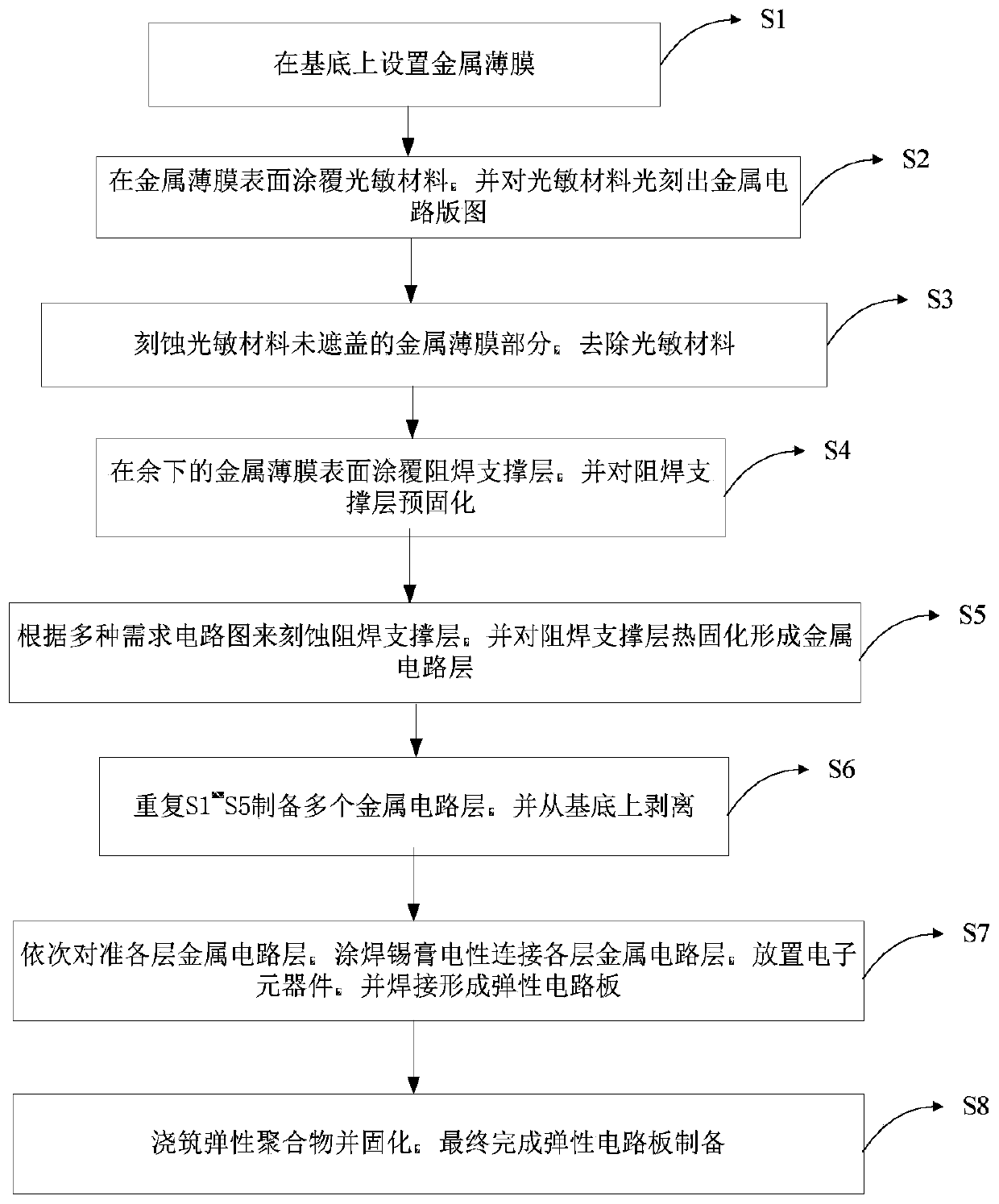
[0047] According to an embodiment of the present invention, a method for preparing a flexible circuit board is provided, see figure 1 , including the following preparation steps:
[0048] S1. setting a metal film 3 on the substrate 1;
[0049] S2. Coating a photosensitive material 4 on the surface of the metal thin film 3, and photoetching a metal circuit layout on the photosensitive material 4;
[0050] S3. Etching the part of the metal film 3 not covered by the photosensitive material 4 to remove the photosensitive material 4;
[0051] S4. Coating a solder resist support layer 5 on the surface of the remaining metal film 3, and pre-curing the solder resist support layer 5; the solder resist support layer 5 needs to meet the required curvature, and can be patterned and insulated at the same time.
[0052] S5. Etching the solder resist support layer 5 according to various required circuit diagrams, and thermally curing the solder resist support layer 5 to form a metal circui...
Embodiment 1
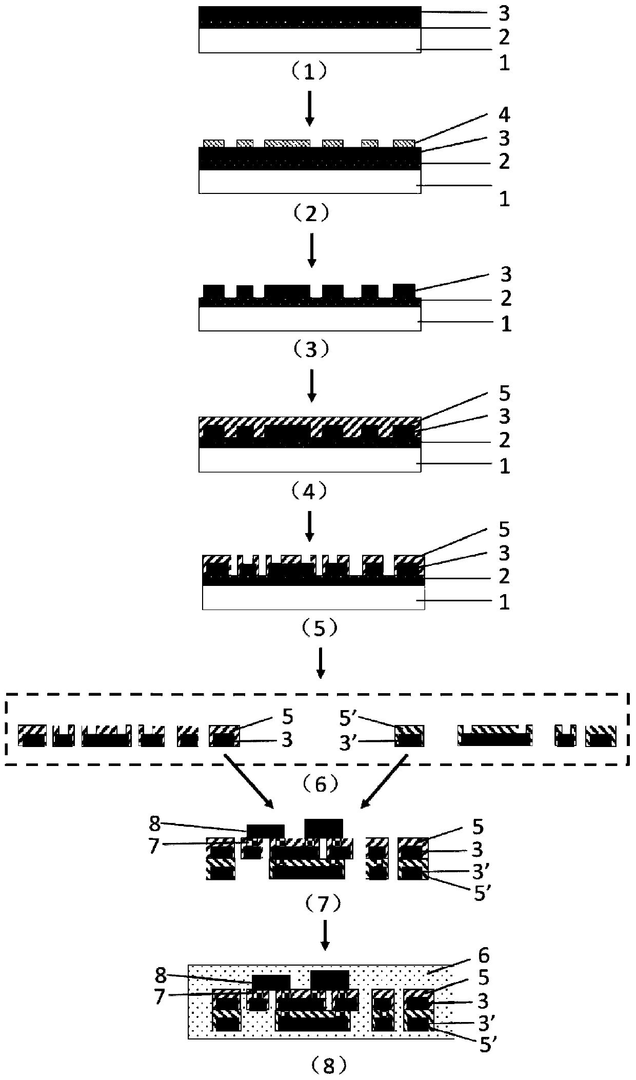
[0059] This embodiment relates to a method for preparing an elastic circuit board. The process flow for preparing the elastic circuit board is as follows: image 3 shown. Utilize the schematic diagram of the cross-section of the elastic circuit board processed by the present invention as Figure 4 As shown, it includes two layers of metal circuit layers, that is, two layers of metal films 3 and 3' and two layers of solder resist support layers 5 and 5', elastic polymer 6, solder paste 7 and a number of electronic components 8; in view of copper Metal has the advantages of low cost, superior electrical properties (low resistivity), easy etching and molding, etc. The metal film 3 and 3' material of this embodiment is copper; considering the copper metal layer thickness of 1 ounce of copper printed circuit board About 35 microns, in order to obtain similar current carrying capacity, the thickness of the metal film 3 and 3' in this embodiment is 40 microns, the minimum line width...
Embodiment 2
[0076] The preparation method of a flexible circuit board involved in this embodiment is the same as that of Embodiment 1, except that the metal film 3 is made of a low-cost aluminum film with a thickness of 10 microns; the minimum line width of the aluminum circuit is 10 microns; The support layer 5 is non-photosensitive polyimide, with a thickness of 15 microns and a minimum line width of 15 microns; the non-photosensitive polyimide solder resist support layer 5 is patterned by dry etching; the elastic polymer 6 It is silicone rubber with good tensile properties and biocompatibility, with a thickness of 1.5mm and 4 metal circuit layers.
PUM
| Property | Measurement | Unit |
|---|---|---|
| thickness | aaaaa | aaaaa |
| thickness | aaaaa | aaaaa |
| thickness | aaaaa | aaaaa |
Abstract
Description
Claims
Application Information


