P-type doped AlScN/AlScN superlattice barrier layer-based efficient light-emitting diode and preparation method

A technology of light-emitting diodes and barrier layers, applied in the field of microelectronics, can solve the problems of increasing the barrier height of hole injection quantum wells, reducing the luminous efficiency of light-emitting diodes, and reducing the efficiency of hole injection, etc., so as to improve performance indicators and increase concentration , The effect of increasing the barrier height

Active Publication Date: 2019-09-10
XIDIAN UNIV
View PDF3 Cites 4 Cited by
  • Summary
  • Abstract
  • Description
  • Claims
  • Application Information

AI Technical Summary

Problems solved by technology

However, since the aluminum composition of the last AlGaN barrier layer is usually smaller than that of the AlGaN electron blocking layer, polarized positive charges will be formed on their interface, and these charges will bend the energy band downwards, forming electron accumulation, making It is easier for electrons to escape the quantum well
At the same time, the electron blocking layer will also increase the barrier height of the hole injection quantum well, resulting in a decrease in the hole injection efficiency.
These problems will lead to the reduction of light-emitting diode luminous efficiency

Method used


Image

  • P-type doped AlScN/AlScN superlattice barrier layer-based efficient light-emitting diode and preparation method
  • P-type doped AlScN/AlScN superlattice barrier layer-based efficient light-emitting diode and preparation method
  • P-type doped AlScN/AlScN superlattice barrier layer-based efficient light-emitting diode and preparation method

Examples


Embodiment 1

[0036] Example 1, preparing a light emitting diode with a light emitting wavelength of 365nm.

[0037] Step 1, pretreating the substrate substrate.

[0038] 1a) After cleaning the gallium oxide substrate, place it in the metal organic chemical vapor deposition MOCVD reaction chamber, and reduce the vacuum degree of the reaction chamber to 3×10 -2 Torr: Introduce hydrogen gas into the reaction chamber, and under the condition that the pressure of the MOCVD reaction chamber reaches 25 Torr, heat the substrate to a temperature of 900°C and keep it for 10 minutes to complete the heat treatment of the substrate;

[0039] 1b) The heat-treated substrate is placed in a reaction chamber with a temperature of 1000° C., and a nitrogen source with a flow rate of 3500 sccm is passed through, and the nitriding is carried out for 3 minutes, and the nitriding is completed.

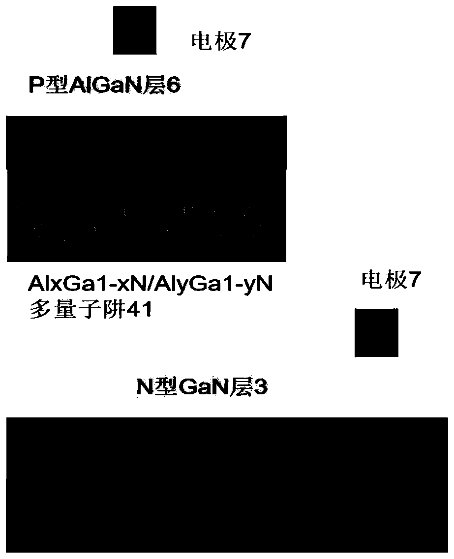
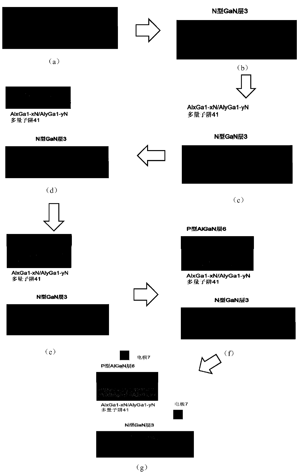
[0040] Step 2, growing a high-temperature AlN layer, such as figure 2 (a).

[0041] On the nitrided substrate, the ...

Embodiment 2

[0054] Example 2, preparing a light emitting diode with a light emitting wavelength of 283nm.

[0055] Step 1, pretreating the substrate substrate.

[0056] The specific implementation of this step is the same as step 1 of embodiment 1.

[0057] Step 2, growing a high temperature AlN layer, such as figure 2 (a).

[0058] On the substrate after nitriding, the MOCVD process is adopted. Under the condition that the temperature of the reaction chamber is 1200°C and the pressure of the MOCVD reaction chamber reaches 340 Torr, a nitrogen source with a flow rate of 3500 sccm and an aluminum source with a flow rate of 30 sccm are introduced simultaneously, and the growth thickness is 30nm high temperature AlN nucleation layer.

[0059] Step 3, grow n-type GaN layer, such as figure 2 (b).

[0060] On the AlN nucleation layer, the MOCVD process was adopted. Under the condition of the reaction chamber temperature of 1300°C, a nitrogen source with a flow rate of 2700 sccm, a galliu...

Embodiment 3

[0074] Example 3, preparing a light emitting diode with a light emitting wavelength of 233nm.

[0075] Step A, pretreating the substrate.

[0076] The specific implementation of this step is the same as step 1 of embodiment 1.

[0077] Step B, growing a high temperature AlN layer, such as figure 2 (a).

[0078] On the substrate after nitriding, the MOCVD process is adopted. Under the conditions of the temperature of the reaction chamber at 1300°C and the pressure of the reaction chamber at 400 Torr, a nitrogen source with a flow rate of 4000 sccm and an aluminum source with a flow rate of 40 sccm are simultaneously introduced, and the growth thickness is 50 nm. high temperature AlN nucleation layer.

[0079] Step C, growing an n-type GaN layer, such as figure 2 (b).

[0080] On the AlN nucleation layer, the MOCVD process was adopted. Under the condition of the reaction chamber temperature of 1500°C, a nitrogen source with a flow rate of 3000 sccm, a gallium source with ...


PUM


Abstract

The invention discloses a P-type doped AlScN/AlScN superlattice barrier layer-based efficient light-emitting diode and preparation method, and mainly solves the problems that an existing p-type regionis low in hole injection efficiency, and electronic leakage exists in a quantum well. The efficient light-emitting diode comprises a gallium oxide substrate layer, a high-temperature AlN nucleating layer and an n-type GaN layer from bottom to top, wherein an electrode and a working region layer are arranged on the n-type GaN layer; an electron blocking layer, a p-type layer and an electrode are sequentially arranged on the upper surface of the working region layer, and the working region layer comprises six periods AlxGa1-xN/AlyGa1-yN multi-quantum-well layer and a barrier layer; and the barrier layer adopts a P-type doped AlmSc1-mN/AlnSc1-nN superlattice structure, so that electron depletion with the electron blocking layer is realized. According to the light-emitting diode, electronic leakage is reduced, the hole injection potential barrier is reduced, the hole concentration in the quantum well is improved, and the light-emitting diode can be used for preparing efficient ultravioletand deep ultraviolet light-emitting equipment.

Description

technical field [0001] The invention belongs to the technical field of microelectronics, and particularly relates to a high-efficiency light-emitting diode, which can be used to manufacture high-efficiency ultraviolet and deep ultraviolet light-emitting devices. [0002] technical background [0003] Since the light-emitting wavelength of AlGaN material can be as short as 200nm, it has become an important material for making ultraviolet and deep ultraviolet light-emitting diodes, and can be widely used in water purification, biological agent detection, sterilization, medicine, etc. [0004] In nitride light-emitting diodes, due to the low ionization rate and low hole mobility of Mg in the p-type layer, and the high ionization rate and high mobility of Si in the n-type layer, it often causes hole injection into quantum wells. Inefficiency and leakage of electrons to the P-type region, this process often causes a reduction in the luminous efficiency of UV LEDs. Therefore, how ...

Claims


Application Information

Patent Timeline
Patent Type & Authority Applications(China)
IPC IPC(8): H01L33/00H01L33/06H01L33/32
CPCH01L33/06H01L33/32H01L33/007
Inventor 张雅超马德璞许晟瑞王学炜张进成马佩军张春福郝跃
Owner XIDIAN UNIV
Why Eureka
Try Eureka