Electro-thermal radiation light emitting array device and preparation method and application thereof

A light-emitting array and thermal radiation technology, applied in the direction of electroluminescent light source, electric light source, electrical components, etc., can solve the problems of easy oxidation of graphene and complicated preparation process, and achieve easy silicon-based process integration, high resolution, The effect of good application prospects

Inactive Publication Date: 2019-10-01
NAT UNIV OF DEFENSE TECH
View PDF2 Cites 6 Cited by
  • Summary
  • Abstract
  • Description
  • Claims
  • Application Information

AI Technical Summary

Problems solved by technology

[0005] The purpose of the present invention is to provide an electrothermal radiation luminescence array device and its preparation method and application in view of the defects that graphene is easily oxidized and the preparation process of graphene thermal radiation luminescence array is complicated in the prior art. The radioluminescent array device is based on the graphene thin film array on the silicon wafer, and makes full use of the insulating properties of aluminum oxide to cover the surface of the graphene thin film array device to isolate it from the air. At the same time, the preparation of the graphene radiation array is relatively Compared with the traditional method, a simpler and more convenient process is adopted

Method used


Image

  • Electro-thermal radiation light emitting array device and preparation method and application thereof
  • Electro-thermal radiation light emitting array device and preparation method and application thereof
  • Electro-thermal radiation light emitting array device and preparation method and application thereof

Examples


Embodiment 1

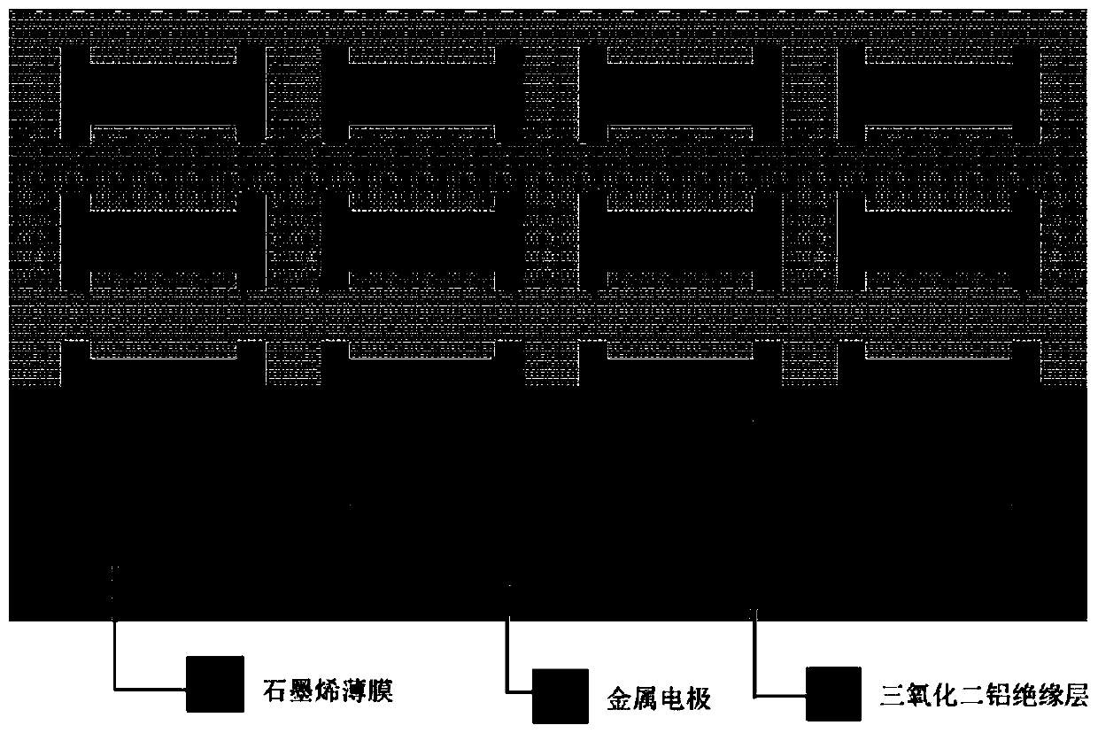
[0049] A method for preparing an electrothermal radiation light-emitting array device, which comprises the following steps:

[0050] S1. Transfer the graphene film to the surface of the silicon wafer:

[0051] S11, spin-coating a polymethyl methacrylate solution layer on the surface of the graphene layer based on the metal foil, and drying;

[0052] S12. After the polymethyl methacrylate is cured, use (NH 4 ) 2 S 2 o 8 Solution etching to remove the metal foil substrate;

[0053] S13, the obtained graphene film having a polymethyl methacrylate layer on the surface is cleaned in deionized water and then picked up with a base silicon wafer and dried;

[0054] S14, using acetone to dissolve the polymethyl methacrylate layer;

[0055] S15. Place the graphene film on the silicon wafer treated in step S14 in a mixture of argon and hydrogen for annealing at 200° C. to remove residual polymethyl methacrylate and solvent acetone on the surface of the graphene.

[0056] S2. Etchi...

Embodiment 2

[0073] The application of the electrothermal radiation light emitting array device obtained in Example 1 in integrated high-speed optical communication, the electrothermal radiation light emitting array device is used as a high-speed, ultra-small light source on a silicon chip.

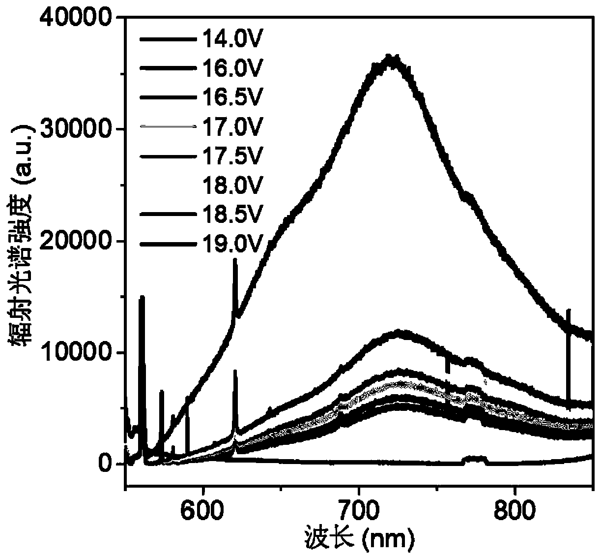
[0074] Connect the electrode of the light-emitting array device to the external circuit through a conductive metal wire by using an ultrasonic pressure welding machine, one end of the electrode is grounded, the other end is connected to a voltage source, and the scanning bias voltage is set to 0V to 30V;

[0075] Using InGaAs-based and Si-based CCD spectrometers to measure the radiative luminescence spectrum of the light-emitting array device under the action of bias voltage, the radiative spectrum is shown in the attached image 3 shown. From the radiation spectrum diagram, we can see that with the increase of the applied source-drain bias voltage, the intensity of the radiation spectrum changes sign...

Embodiment 3

[0079] Application of the electrothermal radiation luminescence array device obtained in Example 1 in an infrared thermal imaging system. The electrothermal radiation emission array device is used for infrared target imaging, and its advantages lie in high resolution and high frame rate. Compared with traditional The silicon-based resistor array analog imaging technology overcomes the shortcomings of the latter, such as slow temperature change, limited temperature range, and multi-spectral range, and can realize infrared target imaging such as simulated high-speed motion and full-band radiation.


PUM

PropertyMeasurementUnit
thicknessaaaaaaaaaa
thicknessaaaaaaaaaa
thicknessaaaaaaaaaa

Abstract

The invention provides an electro-thermal radiation light emitting array device, which comprises a silicon wafer, a graphene film array on the silicon wafer, metal electrodes vapor-plated at the two ends of each graphene film in the graphene film array, and an aluminum oxide insulating layer at the top. The aluminum oxide insulating layer is deposited on the outermost layer of the whole silicon wafer to cover the graphene film array, the metal electrodes and the surface of the silicon wafer outside the area of the graphene film array and the metal electrodes, and are used to isolate the graphene films on the silicon wafer from the air and avoid the oxidation of the graphene films. A preparation method of the device and an application of the device prepared by the method in the field of optical communication are also provided. The electro-thermal radiation light emitting array device of the invention has the advantages of small volume, high resolution, fast switching, adjustable radiation wavelength, large-scale production and easy integration with a silicon-based process, and has a good application prospect in on-chip integrated high-speed optical communication.

Description

technical field [0001] The invention generally belongs to the technical field of preparation and application of electrothermal radiation light emitting devices or graphene nano devices, and in particular relates to an electrothermal radiation light emitting array device and its preparation method and application. Background technique [0002] The rapid development of nanophotonics devices, including waveguides, optical modulators, and photodetectors, has greatly contributed to the advancement of on-chip integrated optical communications over the past few decades. However, as an important part of on-chip integrated photonics: on-chip light source with high-speed modulation function, there are still many challenges. [0003] Graphene is a honeycomb lattice material with a thickness of only one or a few layers of carbon atoms. It has excellent characteristics such as high thermal conductivity, low heat capacity and ultra-fast photoelectric response, and can still maintain a sta...

Claims


Application Information

Patent Timeline
Patent Type & Authority Applications(China)
IPC IPC(8): H05B33/04H05B33/14
CPCH05B33/04H05B33/145
Inventor 朱梦剑罗芳秦石乔
Owner NAT UNIV OF DEFENSE TECH
Why Eureka
Try Eureka