A kind of preparation method of wafer level vanadium dioxide thin film
A vanadium dioxide, wafer-level technology, applied in the field of functional thin film preparation, can solve the problems of narrow oxidation temperature, annealing time and oxygen partial pressure parameter window, obtaining high-quality large-size thin films, and demanding process parameters. , to achieve the effect of efficient preparation, large-scale production and application, and excellent performance
- Summary
- Abstract
- Description
- Claims
- Application Information
AI Technical Summary
Problems solved by technology
Method used
Image

Examples
preparation example Construction
[0035] The invention provides a method for preparing a wafer-level vanadium dioxide film, comprising the following steps:
[0036] S1. Provide a uniformly grown metal vanadium film;
[0037] S2. Using water vapor to oxidize the metal vanadium thin film at a temperature of 450-650° C. under oxygen-free conditions to obtain a monoclinic phase vanadium dioxide thin film.
[0038] The method for preparing the vanadium dioxide thin film is simple, highly repeatable, and low in cost; the prepared vanadium dioxide thin film is uniform and compact, has excellent metal-insulator transition performance, and its size can reach wafer level, which is beneficial for application.
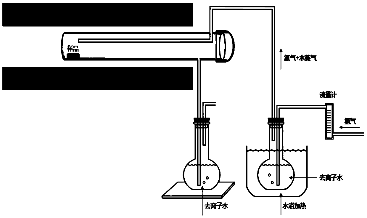
[0039] see figure 1 , figure 1 It is a schematic diagram of a device for growing a vanadium dioxide film by water vapor oxidation in an embodiment of the present invention. In order to solve the problems of harsh experimental conditions and expensive experimental equipment in the existing preparation methods of...
Embodiment 1
[0054] Select a 2 inch diameter round Al 2 o 3 (0001) Substrate, using thermal evaporation method at a vacuum degree better than 4×10 -3 Pa, and then the substrate was rotated at a constant speed of 4 rpm.
[0055] Turn on the electron gun for heating, vaporize the metal vanadium with a purity of 99.99% to produce a vanadium atom beam, measure its rate with a quartz crystal vibrating film thickness meter, and adjust the power of the electron beam evaporation source to produce a stable vanadium atom beam at a rate of 5.5 Angstroms / min. Open the baffle, spray the metal vanadium atom beam onto the surface of the substrate for reaction deposition, grow and form the metal vanadium thin film, and the growth time is 40 minutes.
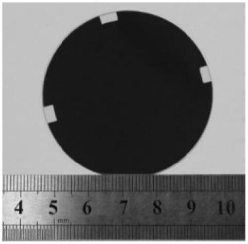
[0056] After the growth process is over, the metal vanadium atomic beam is turned off, and the prepared metal vanadium thin film is taken out from the vacuum chamber. The thickness of the metal vanadium thin film is 20nm, and its actual photo can be foun...
Embodiment 2
[0062] Select a 2 inch diameter round Al 2 o 3 (0001) Substrate, using thermal evaporation method at a vacuum degree better than 5×10 -3 Pa, and then the substrate was rotated at a constant speed of 4 rpm.
[0063] Turn on the electron gun for heating, vaporize the metal vanadium with a purity of 99.99% to produce a vanadium atom beam, measure its rate with a quartz crystal vibrating film thickness meter, and adjust the power of the electron beam evaporation source to produce a stable vanadium atom beam at a rate of 7.5 Angstroms / min. Open the baffle, spray the metal vanadium atom beam onto the surface of the substrate for reaction deposition, grow and form the metal vanadium thin film, and the growth time is 260 minutes.
[0064] After the growth process is over, the metal vanadium atomic beam is turned off, and the prepared metal vanadium film is taken out from the vacuum chamber, and the film thickness is 200 nm.
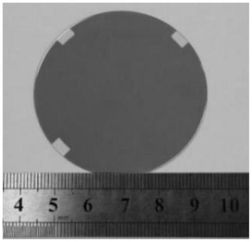
[0065] use figure 1 In the device shown, the metal van...
PUM
| Property | Measurement | Unit |
|---|---|---|
| thickness | aaaaa | aaaaa |
| thickness | aaaaa | aaaaa |
| thickness | aaaaa | aaaaa |
Abstract
Description
Claims
Application Information
 - R&D
- Intellectual Property
- Life Sciences
- Materials
- Tech Scout
- Unparalleled Data Quality
- Higher Quality Content
- 60% Fewer Hallucinations
Browse by: Latest US Patents, China's latest patents, Technical Efficacy Thesaurus, Application Domain, Technology Topic, Popular Technical Reports.
© 2025 PatSnap. All rights reserved.Legal|Privacy policy|Modern Slavery Act Transparency Statement|Sitemap|About US| Contact US: help@patsnap.com