Electroless plating process

A process, nickel-plating technology, applied in the direction of metal material coating process, circuit, printed circuit, etc., to achieve the effect of thin film and excellent packaging characteristics

Active Publication Date: 2019-10-11
KOJIMA CHEM CO LTD
View PDF9 Cites 2 Cited by
  • Summary
  • Abstract
  • Description
  • Claims
  • Application Information

AI Technical Summary

Problems solved by technology

[0005] As the above-mentioned plating treatment, the electrolytic plating process is the mainstream, but for cases where the electrolytic plating process cannot cope, the electroless plating process is applied

Method used


Image

  • Electroless plating process
  • Electroless plating process
  • Electroless plating process

Examples


Embodiment 1

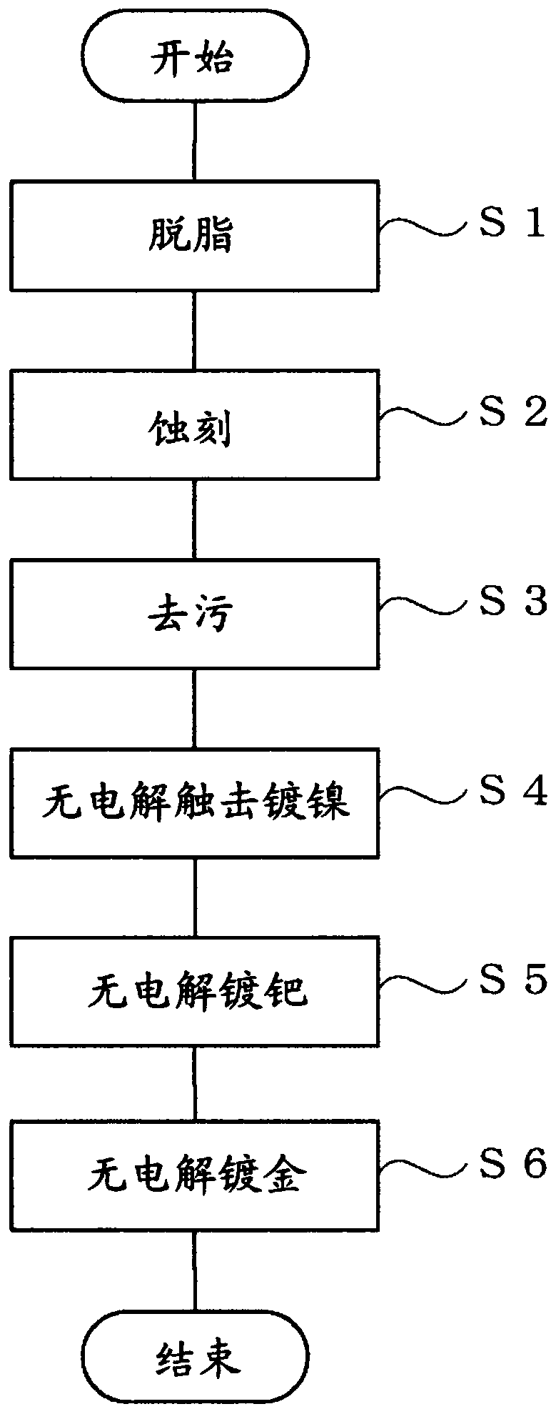
[0089] In the electroless plating process of this embodiment, by sequentially figure 1 In each of the shown steps S1 to S6 (all six steps), a Ni / Pd / Au film is formed on the surface of the copper material. After performing the above-mentioned degreasing step (S1), etching step (S2), and desmearing step (S3) in sequence, an electroless nickel strike plating step (S4) is performed. In the electroless nickel strike plating step ( S4 ), the copper material is immersed in an electroless nickel strike plating solution having the following composition to form a nickel plating film on the surface of the copper material. The electroless nickel strike plating solution is prepared by mixing nickel sulfate hexahydrate, DL-malic acid and water to form an aqueous solution containing a nickel complex, and then adding dimethylamine borane to it and stirring. . While the copper material is immersed in the electroless nickel strike plating solution, the electroless nickel strike plating solut...

reference example 1

[0111] The electroless plating process of this reference example was performed in the same manner as Comparative Example 1 except that the palladium catalyst application treatment ( S14 ) was not performed before the electroless nickel plating ( S15 ). The electroless plating process of this reference example has six steps in total.

reference example 2

[0113] The electroless plating process of this reference example was performed in the same manner as Comparative Example 2 except that the palladium catalyst application treatment (S14) was not performed before the electroless nickel plating (S15).

[0114]

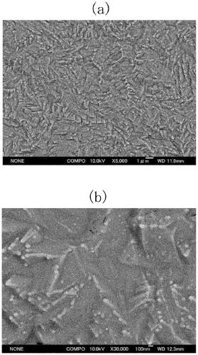
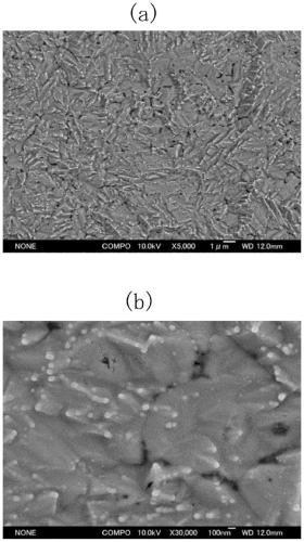
[0115] 1. Evaluation of nickel-plated film

[0116] First, proceed to the electroless nickel strike plating process (S4) of the electroless plating process of Example 1, or proceed to the electroless nickel plating process of the electroless plating process of Comparative Example 1 and Comparative Example 2 (S15) , thereby forming a nickel-plated film with a film thickness of 0.01 μm on the surface of the copper material. The following evaluation was performed about the obtained nickel plating film.

[0117] 1-1. Nickel Precipitation

[0118] Here, a test plate was used in which 30 copper pads with a diameter of 0.45 mm were arranged in a grid at intervals of 30 μm on an insulating base material. Then, proceed to the...


PUM

PropertyMeasurementUnit
thicknessaaaaaaaaaa
thicknessaaaaaaaaaa
thicknessaaaaaaaaaa

Abstract

The purpose of the present invention is to provide an electroless plating process which is capable of obtaining a film equipped with excellent mounting properties and capable of making the thickness of the nickel plating film thin when a nickel plating film and a gold plating film are formed in this order on the surface of a copper material. This electroless plating process for forming a nickel plating film and a gold plating film in this order on the surface of a copper material by using an electroless plating method is characterized by being provided with a step for forming a nickel platingfilm on the surface of a copper material by using an electroless strike plating method, and a step for forming a gold plating film by using a reduction-type electroless plating method.

Description

technical field [0001] The invention relates to an electroless plating process for forming a gold-plated film on the surface of a copper material by an electroless plating method. Background technique [0002] In recent years, on the one hand, the demand for high-function and multi-functionalization of electronic equipment has increased, and on the other hand, electronic circuit substrates such as resin substrates, ceramic substrates, and chip substrates used in these electronic devices also need to be further thinned and shortened. Since high-density packaging is required to cope with this reduction in weight and size, a surface treatment technology capable of achieving high-density packaging is required. Furthermore, in the technical field of electronic circuit boards, a packaging technique using solder or wire bonding has been established as a technique for joining packaged components. [0003] In order to ensure connection reliability during packaging, the wiring pad, w...

Claims


Application Information

Patent Timeline
Patent Type & Authority Applications(China)
IPC IPC(8): C23C18/52C23C18/34H01L21/28H01L21/288H01L21/3205H01L21/768H01L23/522H01L23/532H05K3/18
CPCC23C18/34C23C18/1651C23C18/1694C23C18/44C23C18/1844H01L24/00H01L2224/48227H01L2224/16225H01L2224/13101H01L2224/81444H01L2224/85444H01L2224/45144H01L2224/45015H01L24/48H01L24/16H01L24/81H01L24/85H01L24/45H01L21/48H05K3/244H05K2201/0338H05K2203/072H05K2203/073H05K2203/0789H01L2924/014H01L2924/00014H01L2924/20752C23C18/52C23C18/1637H01L21/7685H01L21/76874
Inventor 加藤友人渡边秀人
Owner KOJIMA CHEM CO LTD
Why Eureka
Try Eureka