A two-dimensional high conductivity hydrogenated nbse 2 Nano film, its preparation method and application
A high-conductivity, nano-thin film technology, applied in the field of materials, can solve problems such as limited application of two-dimensional materials
- Summary
- Abstract
- Description
- Claims
- Application Information
AI Technical Summary
Problems solved by technology
Method used
Image

Examples
preparation example Construction
[0029] The invention provides a two-dimensional high conductivity hydrogenated NbSe 2 A method for preparing nanosheets, comprising:
[0030] A) Layered NbSe 2 The block is immersed in the lithium source solution to react to obtain the precursor Li x NbSe 2 ;
[0031] B) will Li x NbSe 2 Dispersed in deionized water, protected by inert gas, and ultrasonically stripped to obtain dispersed ultra-thin two-dimensional high-conductivity hydrogenated H x NbSe 2 Nanosheets.
[0032] Two-dimensional high conductivity hydrogenated NbSe provided by the present invention 2 The nanosheets first layered NbSe 2 The block is immersed in the lithium source solution to react to obtain the precursor Li x NbSe 2 .
[0033] The present invention firstly prepares layered NbSe 2 The block material is not limited in the present invention, and commercially available ones can be used. Preferably its size is 5 to 10 mm.
[0034] The lithium source of the present invention is an organolit...
Embodiment 1
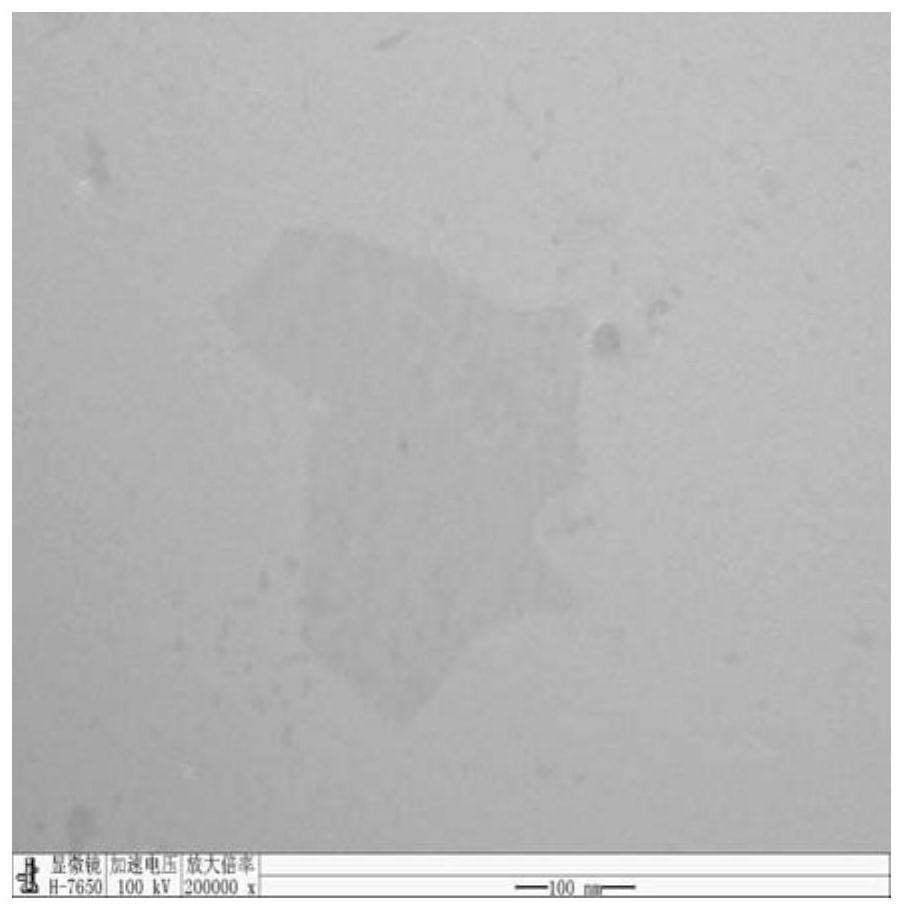
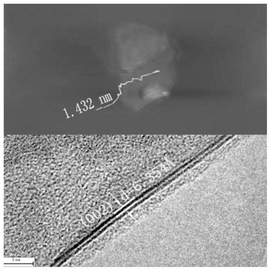
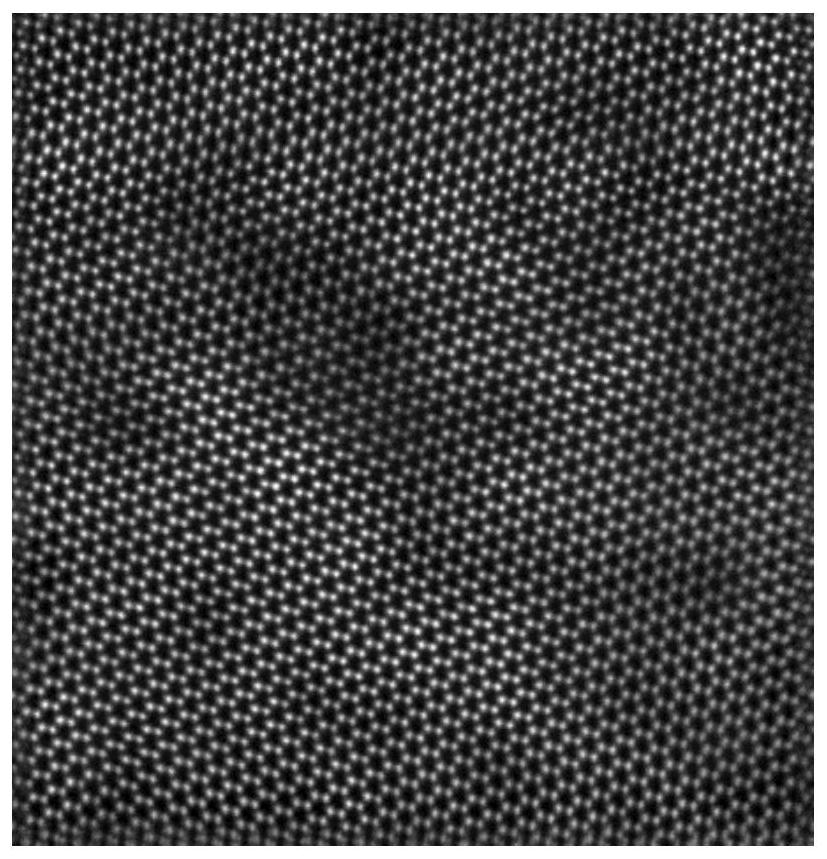
[0061] At normal pressure, the layered NbSe 2 The block was soaked in a hexane solution of n-butyllithium at 80°C for 3 hours to prepare the precursor Li x NbSe 2 ; Will Li x NbSe 2 Dispersed in deionized water, protected by nitrogen gas, and ultrasonically stripped for 30 minutes to obtain dispersed ultra-thin HxNbSe 2 nanosheets; ultrathin H x NbSe 2 The size of the nano sheet is 1-50 μm, and the thickness is less than 1 nm. figure 1 Electron micrograph of the nanosheets prepared in Example 1 of the present invention, figure 2 The atomic force scanning and electron microscope cross-sectional photos of the nanosheets prepared in Example 1 of the present invention, image 3 It is a high-resolution atomic phase picture of the nanosheets prepared in Example 1 of the present invention.
Embodiment 2
[0063] At normal pressure, the layered NbSe 2 The block was soaked in a hexane solution of n-butyllithium at 80°C for 3 hours to prepare the precursor Li x NbSe 2 ; Will Li x NbSe 2 Dispersed in deionized water, protected by nitrogen gas, and ultrasonically stripped for 50 minutes to obtain dispersed ultra-thin HxNbSe 2 nanosheets; ultrathin H x NbSe 2 The size of the nano sheet is 1-50 μm, and the thickness is less than 1 nm.
[0064] The crystal quality and phase of the prepared nanosheets can be analyzed by X-ray diffractometer, such as Figure 4 As shown, the X-ray diffraction image shows that the obtained nanosheet samples are highly crystalline and oriented, and the pattern is consistent with the metallic phase NbSe at room temperature 2 X-ray diffraction c-direction orientation spectrum.
PUM
| Property | Measurement | Unit |
|---|---|---|
| size | aaaaa | aaaaa |
| thickness | aaaaa | aaaaa |
| pore size | aaaaa | aaaaa |
Abstract
Description
Claims
Application Information
 - R&D
- Intellectual Property
- Life Sciences
- Materials
- Tech Scout
- Unparalleled Data Quality
- Higher Quality Content
- 60% Fewer Hallucinations
Browse by: Latest US Patents, China's latest patents, Technical Efficacy Thesaurus, Application Domain, Technology Topic, Popular Technical Reports.
© 2025 PatSnap. All rights reserved.Legal|Privacy policy|Modern Slavery Act Transparency Statement|Sitemap|About US| Contact US: help@patsnap.com