A method of measuring the change of charge density on the surface of wafer

A surface charge density, wafer technology, applied in the measurement of electrical variables, measurement devices, semiconductor/solid-state device testing/measurement, etc., can solve the problem of high cost of surface charge measurement, achieve fast measurement, simple calculation method, simple structure Effect

Active Publication Date: 2021-07-09
JIANGSU MICROVIA NANO EQUIP TECH CO LTD
View PDF6 Cites 0 Cited by
  • Summary
  • Abstract
  • Description
  • Claims
  • Application Information

AI Technical Summary

Problems solved by technology

[0004] In order to solve the technical problem of high cost of surface charge measurement in the prior art, the patent of this invention proposes a fast measurement, simple calculation method, and strong robustness, which can be used as an on-line monitor to indicate film quality in semiconductor production and research and development. method

Method used


Image

  • A method of measuring the change of charge density on the surface of wafer
  • A method of measuring the change of charge density on the surface of wafer
  • A method of measuring the change of charge density on the surface of wafer

Examples


Embodiment Construction

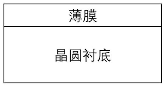
[0041] The present invention takes the P-type single-sided polished silicon wafer as an example, below in conjunction with the attached figure 2 The technical solution of the present invention is described in detail.

[0042] P-type single-sided polished silicon wafer, the resistivity is about 3000Ω-cm, the thickness is 400±20μm, and the crystal orientation silicon wafer size is 50.8±0.2mm in diameter. The surface of the silicon wafer is clean but has a natural oxide layer, which contains negligible surface charges.

[0043] The surface sheet resistance of the polished surface of the silicon wafer before film deposition was measured by four-probe measurement method to be 8.0±1.0×10 5 Ω / sq., corresponding to R in formula (4) 0 .

[0044] Aluminum oxide (AlO) with a thickness of about 15 nm was deposited by atomic layer deposition (ALD) x ) film on the polished surface of the silicon wafer. Measure the sheet resistance of the silicon wafer surface to be 6.5±0.5×10 4 Ω / sq....


PUM

PropertyMeasurementUnit
thicknessaaaaaaaaaa
thicknessaaaaaaaaaa
diameteraaaaaaaaaa

Abstract

The invention discloses a method for measuring the change of charge density on the surface of a wafer: measuring the surface sheet resistance (denoted as R 0 ); after depositing a thin film on the surface of the wafer (or after the deposited film has been processed by a certain process), measure the sheet resistance of the wafer surface (denoted as R). If a P-type wafer substrate is used, then the surface charge density change value is ΔQ=-(1 / R-1 / R 0 ) / eμ p ; If an N-type wafer substrate is used, then the surface charge density change value is ΔQ=(1 / R‑1 / R 0 ) / eμ n , where the polarity of the charge change is given by the positive and negative values ​​of the formula: a positive value represents an increase in positive charge or a decrease in negative charge; a negative value represents an increase in negative charge or a decrease in positive charge, where e is the elementary charge; μ p and μ n are hole mobility and electron mobility, respectively, and the two are fixed values ​​for the specific wafer used.

Description

technical field [0001] The invention relates to the analysis and detection of the fixed charge density inside the thin film and / or the interface between the thin film and the wafer, involving functional thin films deposited on the surface of wafers in the fields of semiconductor transistor manufacturing and optoelectronic device manufacturing. Background technique [0002] Oxide films such as silicon oxide, aluminum oxide, zirconia, and hafnium oxide, nitride films such as silicon nitride and titanium nitride, and amorphous semiconductor films such as amorphous silicon and amorphous silicon oxide are currently widely used in crystalline semiconductors. Passivation layers for solar cells and as insulating layers in metal-oxide-semiconductor (MOS) field effect transistors are deposited directly on the wafer surface. The fixed charges contained in these thin films and on the interface between the thin film and the wafer can have a significant impact on device performance. Real...

Claims


Application Information

Patent Timeline
Patent Type & Authority Patents(China)
IPC IPC(8): H01L21/66G01R29/24
CPCG01R29/24H01L22/14H01L22/20
Inventor 张鹤李翔黎微明
Owner JIANGSU MICROVIA NANO EQUIP TECH CO LTD
Why Eureka
Try Eureka