
Gallium arsenide single crystal growth device and growth method

A growth device and growth method technology, applied in the field of crystal growth, can solve the problems of inability to grow single crystals, long growth cycle, high cost, reduce material loss, impurity pollution, good single crystal performance and quality, and reduce processing and cleaning. Effect

Active Publication Date: 2019-10-22
FIRST SEMICON MATERIALS
View PDF9 Cites 5 Cited by
  • Summary
  • Abstract
  • Description
  • Claims
  • Application Information

AI Technical Summary

Problems solved by technology

[0003] At present, the mature VGF method of GaAs single crystal growth process is relatively complicated, and cannot grow single crystals from raw materials arsenic and gallium in one step. Firstly, 6N arsenic and 6N gallium are synthesized into GaAs polycrystalline material by horizontal Bridgman method, and then The GaAs polycrystalline material is processed into a specified shape, and then cleaned and put into a pyrolytic boron nitride (PBN) crucible, and then the GaAs polycrystalline material is sealed by vacuuming and other methods, and by adding B 2 o 3 As a liquid sealant and wetting agent to form the boundary conditions required for GaAs single crystal growth
With the existing VGF single crystal growth process, the growth cycle is long. From the synthesis of gallium arsenide polycrystalline materials to the growth of single crystals, a large amount of materials are lost, and other impurities are also brought in, which affect the survival rate of single crystals.
The growth process of this process is complex, the cycle is long, the loss of materials is large, and the cost is high

Method used


Image

  • Gallium arsenide single crystal growth device and growth method
  • Gallium arsenide single crystal growth device and growth method
  • Gallium arsenide single crystal growth device and growth method

Examples


Embodiment 1

[0042] An embodiment of the gallium arsenide single crystal growth method of the present invention uses the gallium arsenide single crystal growth device of the present invention for single crystal growth.

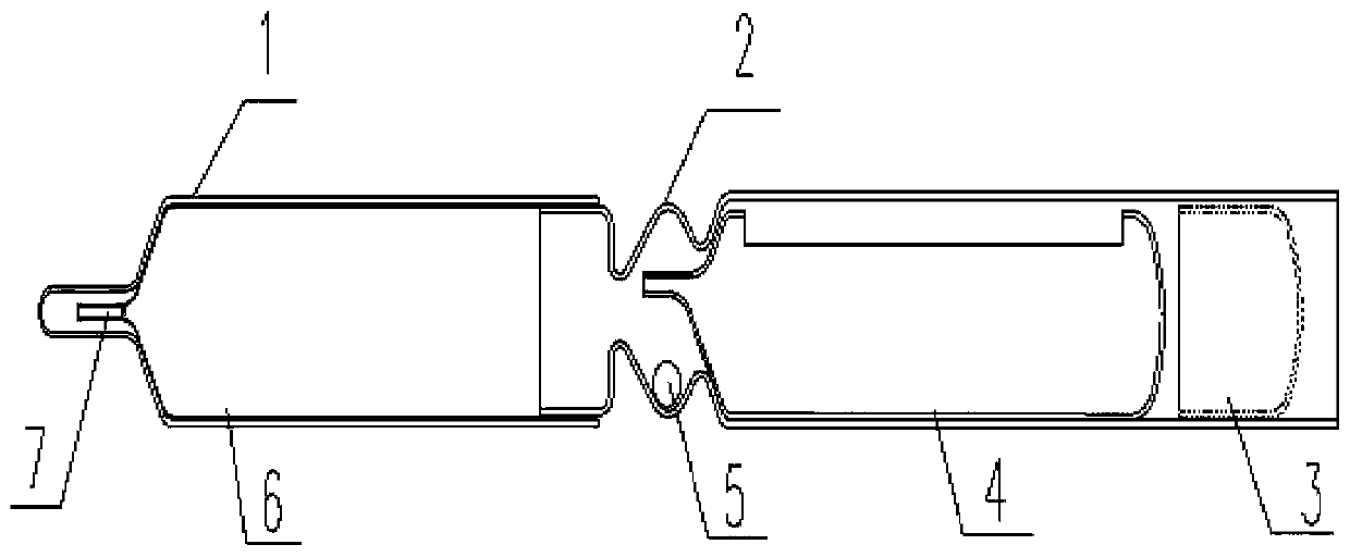
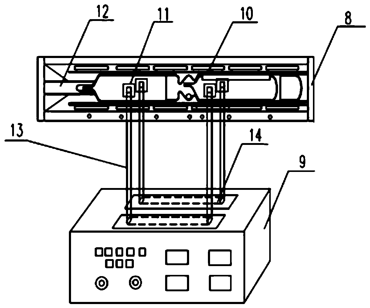
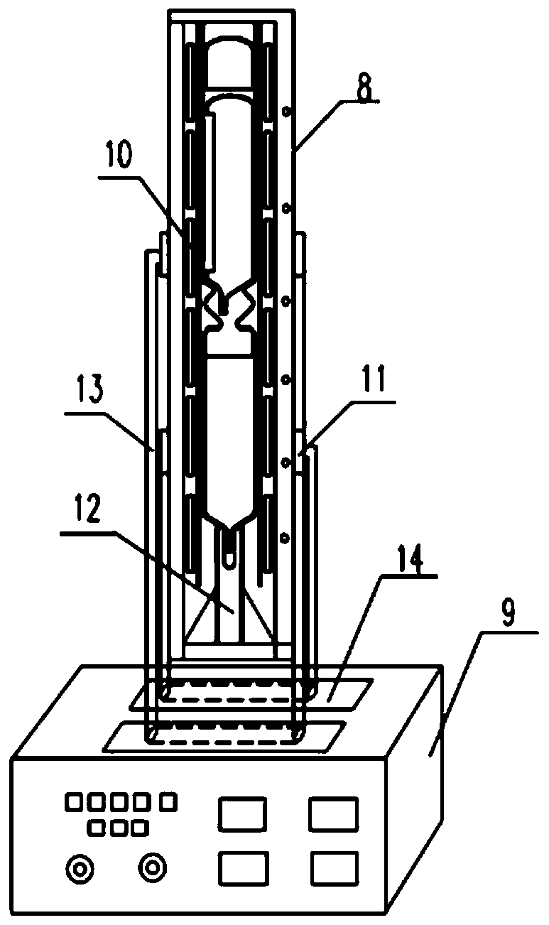
[0043] The specific structure of the gallium arsenide single crystal growth device of the present invention is: including quartz tube parts, single crystal furnace body, single crystal furnace frame, controller, heating wire, quartz support tube, furnace lifting rod, lifting rod slideway , the quartz tube part is set in the body of the single crystal furnace, the body of the single crystal furnace is placed on the frame of the single crystal furnace, the slideway of the lifting rod is set on the upper part of the controller, and the controller slides through the lifting rod The road is connected with the furnace body lifting rod, and the furnace body lifting rod is connected with the single crystal furnace body through the single crystal furnace frame, and the single crysta...

Embodiment 2

[0060] An embodiment of the gallium arsenide single crystal growth method of the present invention uses the same gallium arsenide single crystal growth device as in embodiment 1.

[0061] The method for growing a gallium arsenide single crystal in this embodiment includes the following steps:

[0062] (1) Place the gallium arsenide seed crystal in the PBN crucible seed crystal cavity, and then put the PBN crucible into the single crystal quartz tube;

[0063] (2) Butt the head of the W-shaped polycrystalline quartz tube with the tail of the single crystal quartz tube, and then weld the two together with a hydrogen-oxygen flame;

[0064] (3) load 6N arsenic into the welded monocrystalline quartz tube PBN crucible, weight is 5.75Kg, put 40g boron oxide and doped Si sheet into the W-shaped position of W-shaped polycrystalline quartz tube;

[0065] (4) 6N gallium with a weight of 5.3Kg is packed in a quartz boat, then put into a W-shaped polycrystalline quartz tube, and then put ...

Embodiment 3

[0076] An embodiment of the gallium arsenide single crystal growth method of the present invention uses the same gallium arsenide single crystal growth device as in embodiment 1.

[0077] The method for growing a gallium arsenide single crystal in this embodiment includes the following steps:

[0078] (1) Place the gallium arsenide seed crystal in the PBN crucible seed crystal cavity, and then put the PBN crucible into the single crystal quartz tube;

[0079] (2) Butt the head of the W-shaped polycrystalline quartz tube with the tail of the single crystal quartz tube, and then weld the two together with a hydrogen-oxygen flame;

[0080] (3) load 6N arsenic into the welded single crystal quartz tube PBN crucible, weight is 6.25Kg, put 40g boron oxide and doped Si sheet into the W-shaped position of W-shaped polycrystalline quartz tube;

[0081] (4) 6N gallium with a weight of 5.8Kg is packed in a quartz boat, then put into a W-shaped polycrystalline quartz tube, and then put i...


PUM


Abstract

The invention relates to a gallium arsenide single crystal growth device and a growth method, belonging to the field of crystal growth. The gallium arsenide single crystal growth device realizes an integrated single crystal growth process from arsenic and gallium raw materials to gallium arsenide single crystals by improving of the shape of a quartz tube and the structure of a single crystal furnace. The quartz tube component comprises a single crystal quartz tube and a W-shaped polycrystalline quartz tube which are welded together, then charged, then vacuumized, welded and sealed by a quartzcap; and the single crystal furnace is transformed into a horizontal and vertical conversion furnace body. The furnace body is slowly controlled to be vertical from a horizontal shape through. When insynthesizing of polycrystals, the furnace body is horizontal, and when in growing of single crystals, the furnace body is rotated into a vertical shape. Then qualified single crystal is grown throughtemperature control. The method reduces the procedures of gallium arsenide polycrystalline synthesis and single crystal growth, and shortens the single crystal growth time, and the grown single crystal has fewer impurities, better performance and quality and higher crystal formation rate.

Description

technical field [0001] The invention relates to a gallium arsenide single crystal growth device and a growth method, belonging to the field of crystal growth. Background technique [0002] Gallium arsenide (GaAs) is the second-generation semiconductor material after germanium and silicon. The methods used to mass produce GaAs crystals include the traditional liquid-enclosed Czochralski method (LEC method) and the horizontal boat production method (HB method). At the same time, the vertical gradient solidification method (VGF method), the vertical Bridgman method (VB method) and the vapor pressure controlled Czochralski method (VCG method) which have the advantages of the above two methods have also been developed, and 4~ 6 inch large diameter GaAs crystal. [0003] At present, the mature VGF method of GaAs single crystal growth process is relatively complicated, and cannot grow single crystals from raw materials arsenic and gallium in one step. Firstly, 6N arsenic and 6N g...

Claims


Application Information

Patent Timeline
IPC IPC(8): C30B29/42C30B11/00
CPCC30B11/00C30B29/42
Inventor 王金灵周铁军严卫东马金峰
Owner FIRST SEMICON MATERIALS
Learn More