Digital X-ray image detector and preparation method thereof

An image detector and X-ray technology, applied in the field of photodetectors, can solve problems such as image contrast reduction and image quality impact, and achieve the effects of improving image quality, eliminating crosstalk and improving transmission efficiency.

Inactive Publication Date: 2019-11-05
SHENZHEN UNIV
View PDF4 Cites 5 Cited by
  • Summary
  • Abstract
  • Description
  • Claims
  • Application Information

AI Technical Summary

Problems solved by technology

[0006] In view of the above-mentioned deficiencies in the prior art, the object of the present invention is to provide a digital X-ray image detector and its preparation method, aiming to solve the probl

Method used


Image

  • Digital X-ray image detector and preparation method thereof
  • Digital X-ray image detector and preparation method thereof
  • Digital X-ray image detector and preparation method thereof

Examples


preparation example Construction

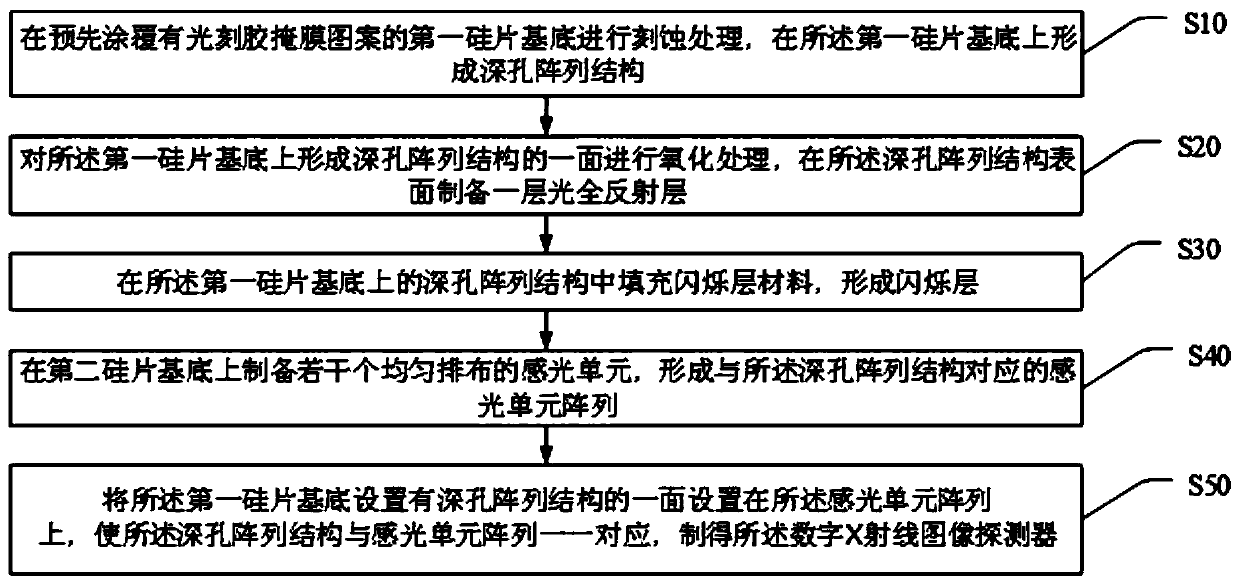
[0038] Further, the present invention also provides a method for preparing a digital X-ray image detector, wherein, as image 3 shown, including steps:

[0039] S10, performing an etching process on the first silicon substrate coated with a photoresist mask pattern in advance, forming a deep hole array structure on the first silicon substrate;

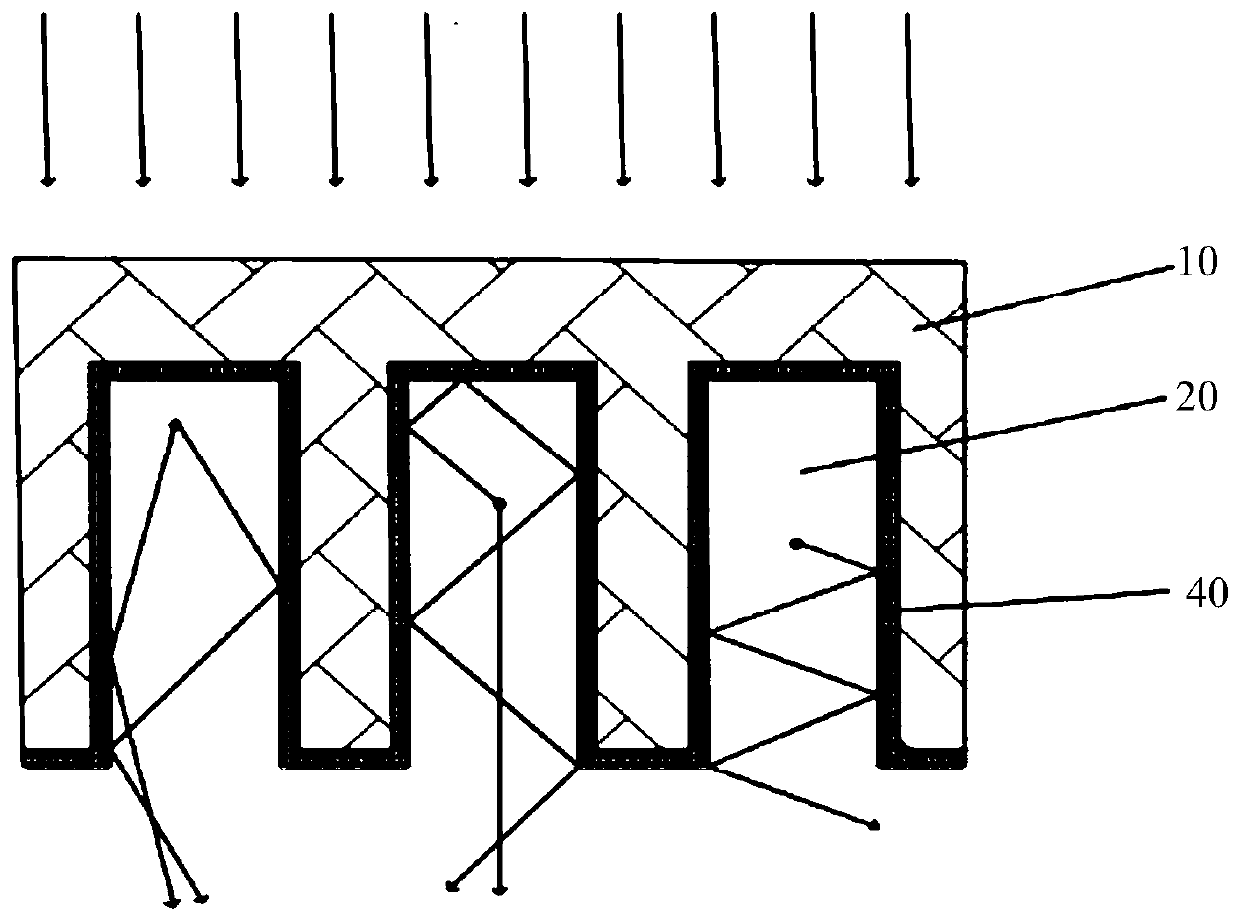
[0040] S20, processing the side on which the deep hole array structure is formed on the first silicon wafer substrate, preparing a layer of light total reflection layer on the surface of the deep hole array structure;

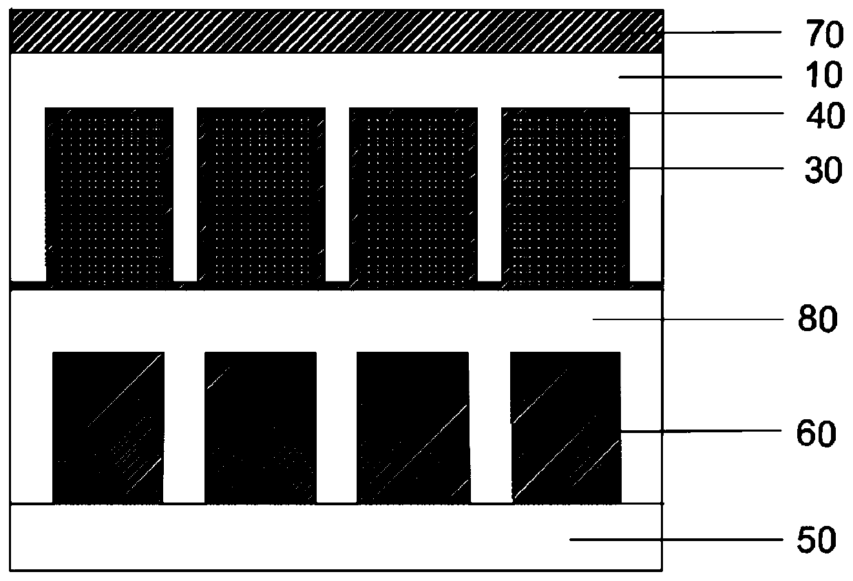
[0041] S30, filling the scintillation layer material in the deep hole array structure on the first silicon wafer substrate to form a scintillation layer;

[0042] S40, preparing several uniformly arranged photosensitive units on the second silicon wafer substrate to form a photosensitive unit array corresponding to the deep hole array structure;

[0043] S50. Place the side of the first silicon wafer substrate provide...

Embodiment 1

[0050] 1) Clean the double-sided polished N-type single crystal silicon wafer with acetone, absolute ethanol, and pure water to remove the stains on the surface; drop a drop of pure water on the silicon wafer, tilt the silicon wafer, and watch whether the pure water drops , if pure water drops, use a plasma cleaning machine to clean the silicon wafer again to increase the hydrophilicity of the silicon wafer;

[0051] 2) Perform coating, photolithography, and development on the cleaned silicon wafer to obtain a mask pattern;

[0052] 3) Aluminum grid structure is distilled on the back of the silicon wafer as an ohmic contact to ensure the uniformity of the electric field on the back of the silicon wafer, and the silicon wafer is immersed in an alkaline solution to form an inverted pyramid structure;

[0053] 4), silicon wafer is put into hydrofluoric acid solution, under the action of applied electric field, carry out the light-assisted electrochemical etching process in wet et...

Embodiment 2

[0059] 1), cleaning the P-type silicon wafer, uniform glue, photolithography and development, to obtain the mask pattern;

[0060] 2), etch the silicon wafer with the mask pattern obtained by dry etching, such as reactive ion etching (RIE), deep reactive ion etching (DRIE), etc., to form a deep hole array structure, and etch to obtain cleaning of the structure;

[0061] 3), process the cleaned silicon wafer with an atomic layer deposition device (ALD), and form an oxide film within 10nm on the inner wall of the deep hole structure (such as SiO 2 ,Al 2 o 3 etc.) or precious metal (e.g. nickel, rhodium, palladium, etc.) thin films;

[0062] 4), filling the deep hole array structure with a perovskite material to form a scintillation layer;

[0063] 5), remove the photoresist and make a one-to-one correspondence between the scintillation layer and the detection unit;

[0064] 6), preparing a layer of protective layer on the upper surface of the silicon chip with the deep hole...


PUM

PropertyMeasurementUnit
Feature sizeaaaaaaaaaa
Depthaaaaaaaaaa

Abstract

The invention discloses a digital X-ray image detector and a preparation method thereof. The digital X-ray image detector comprises a first silicon wafer substrate, a deep hole structure array arranged on the lower surface of the first silicon wafer substrate, scintillation layers loaded in the deep hole structure array and a light total reflection layer arranged between the deep hole structure array and the scintillation layers, wherein the lower surface of the first silicon wafer substrate is correspondingly provided with a second silicon wafer substrate, and the second silicon wafer substrate is provided with a light sensing unit array corresponding to the deep hole structure array. According to the invention, the scintillation layers are arranged in the deep hole array structure, so that the crosstalk phenomenon of visible light between pin columns is eliminated, the generated visible light is enabled to be propagated in a total reflection mode at the interface of the scintillationlayers and the light total reflection layer, and the visible light transmission efficiency is improved. Meanwhile, the scintillation layers in the deep hole array structure are in one-to-one correspondence with the light sensing units in the light sensing unit array, so that the visible light generated by the scintillation layers is enabled to be acquired by the corresponding light sensing unitsto be greater extent, and the image quality is improved.

Description

technical field [0001] The invention relates to the field of photodetectors, in particular to a digital X-ray image detector and a preparation method thereof. Background technique [0002] Due to the strong penetrability of X-rays, X-ray imaging methods are widely used in medical diagnosis and industrial non-destructive testing. In the more than 100 years since the discovery of X-rays, X-ray detection components have also been continuously updated, from the original photosensitive film to the current digital image detector. Common detectors can be divided into two methods: indirect detection and direct detection. Direct detection is to directly convert X-ray images into electrical signals, while indirect detection is to convert X-ray signals into visible light, and then convert visible light into electrical signals. Since indirect detection is superior to direct detection in terms of performance cost and manufacturing area, the current mainstream detection method is indirec...

Claims


Application Information

Patent Timeline
IPC IPC(8): H01L31/08H01L31/18
CPCH01L31/085H01L31/1804Y02P70/50
Inventor 郭金川文明宗方轲杨君
Owner SHENZHEN UNIV
Why Eureka
Try Eureka