SERS substrate based on Au @ Ag nanoparticle ordered array as well as preparation method and application thereof
An ordered array and nanoparticle technology, applied in the field of SERS substrate materials, can solve the problems of difficulty in obtaining large-area regular and ordered array morphology, limiting the application of nanomaterials, and poor SERS enhancement effects, etc., to achieve increased uniformity and The effect of stability, firm combination, and high stability detection
- Summary
- Abstract
- Description
- Claims
- Application Information
AI Technical Summary
Problems solved by technology
Method used
Image
Examples
preparation example Construction
[0027] A method for preparing a SERS substrate based on an ordered array of Au@Ag nanoparticles may include the following steps:
[0028] Step A, preparing a silicon wafer-based single-layer polymer colloidal crystal array, and using the silicon wafer-based single-layer polymer colloidal crystal array as a template, depositing a layer with a thickness of 20 to 40 nm on the surface of the template by using a physical deposition method Au film.
[0029] Step B. Thermally decompose and anneal the template deposited with the Au film to remove the single-layer polymer colloidal crystal array, and at the same time melt, fuse and solidify the Au film in situ, thereby preparing silicon wafer-based two-dimensional Au nanoparticles array.
[0030] Step C, placing the silicon chip-based two-dimensional Au nanoparticle array face up in a citrate buffer solution, then adding 0.1 mol / L silver nitrate solution, and reacting at room temperature for 20 to 30 minutes under dark conditions, Th...
Embodiment 1
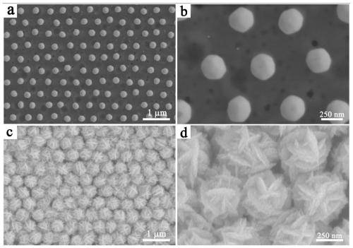
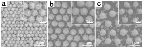
[0046] like Image 6 As shown, a SERS substrate based on an ordered array of Au@Ag nanoparticles, its preparation method may include the following steps:
[0047] Step a, using the gas-liquid interface self-assembly method to prepare a silicon wafer-based single-layer polystyrene colloidal sphere array, and using the silicon wafer-based single-layer polystyrene colloidal sphere array as a template, using a magnetron sputtering deposition method (the processing electric current of magnetron sputtering deposition is 20mA, and processing time is 3~5min, and the gold content of the gold target material used in magnetron sputtering deposition is 99.99%) Deposit a layer thickness on the surface of described template to be 20~5min. 40nm Au film.
[0048] Step b. Put the template deposited with the Au film into a tube furnace, and anneal it in an air atmosphere at 900-1000°C for 2 hours, so that the single-layer polymer colloidal crystal array is thermally decomposed, and at the same...
PUM
 Abstract
Description
Claims
Application Information


