An upright few-layer graphene-metal nanoparticle composite catalytic electrode
A metal nanoparticle, few-layer graphene technology, applied in the field of electrochemistry, can solve the problems of difficult to control the size and morphology of nanoparticles, complicated preparation steps, etc., achieve good and stable physical and chemical properties, simple preparation steps, size and shape. controllable effect
- Summary
- Abstract
- Description
- Claims
- Application Information
AI Technical Summary
Problems solved by technology
Method used
Image
Examples
Embodiment 1
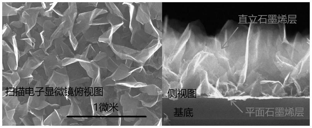
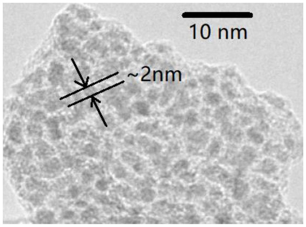
[0037] Such as figure 1 As shown, vertical few-layer graphene has a unique morphology: carbon nanosheets grow vertically and have a large surface area. figure 2 It is revealed that the edge thickness is between 0.34 and 0.37 nm, and it is a graphene structure with one to two layers. image 3 It shows that the size and shape of platinum particles are uniform, and the average diameter is about 2 nanometers.
[0038] A kind of preparation method of upright few-layer graphene-metal nanoparticle composite catalytic electrode, comprises the following steps at least:
[0039] In the first step, put the high-conductivity carbon paper into the vacuum chamber of the plasma chemical vapor deposition device, feed the reducing gas hydrogen and argon at 1:1, and maintain the low pressure state in the device through flow adjustment, so that the vacuum degree is stable at 15Pa, perform plasma etching reaction on the substrate, the reaction time is 10min, and the power density of the plasma...
Embodiment 2
[0047] Different from Example 1 is the preparation method and application of gold nanoparticles on the surface of upright graphene, the method at least includes the following steps:
[0048] In the first step, the gold target is selected, and the material prepared in the first step to the third step in Example 1 is placed in a physical vapor deposition device, and the vacuum is evacuated to 3×10 -3 Pa, filled with argon to stabilize the pressure at 5pa, start magnetron sputtering, where the power is 5W / cm 2 , time 300s;
[0049] In the second step, after the magnetron sputtering is finished, flush argon to 1x10 5 Pa, raise the temperature to 450°C and keep it for 40min for annealing;
[0050] In the third step, after the annealing reaction is completed, the temperature in the equipment drops to room temperature, and the sample is taken out;
[0051] After testing, in this embodiment, gold nanoparticles with a particle diameter of about 13 nm are loaded on the upright graphe...
Embodiment 3
[0053] Different from Examples 1 and 2 are the preparation method and application of the silver nanoparticles on the surface of the upright graphene, the method at least includes the following steps:
[0054] The first step is to select a silver target and place the material prepared in the first step to the third step in Example 1 in a physical vapor deposition device, and vacuumize to 2×10 -3 Pa, filled with argon to stabilize the pressure at 5.2pa, start magnetron sputtering, the power is 4W / cm 2 , time 240s;
[0055] In the second step, after the magnetron sputtering is finished, argon gas is injected to 1×10 5 pa, raise the temperature to 250°C and keep it for 30min for annealing;
[0056] In the third step, after the annealing reaction is completed, the temperature in the equipment drops to room temperature, and the sample is taken out.
[0057] After testing, in this embodiment, the vertical graphene supports nano-silver particles with a particle diameter of about 5 ...
PUM
| Property | Measurement | Unit |
|---|---|---|
| thickness | aaaaa | aaaaa |
| height | aaaaa | aaaaa |
| thickness | aaaaa | aaaaa |
Abstract
Description
Claims
Application Information


