
Eureka
For R&D, Eureka makes reading and utilizing patents & technical documents easy.
Eureka AIR
Designed for self-driven R&D workflows. Generate viable solutions, solve complex R&D challenges, empower your innovation with AI.

Eureka Materials
Designed for material experts only. Revolutionize your material R&D, from search, analyze, to developing new materials.

TechResearch
Generate reliable direction feasibility study reports for your R&D in just a few steps.

TechSeek
Discover and master advanced knowledge NOW. Basics, ideas, possibilities, all at once.

TechMind
As an expert in R&D Theories, TechMind can generates customized viable solutions instantly.

TechRisk
Analyze your overall solution with one click, know your potential R&D risks in advance.

TechMonitor
Get weekly tech updates, stay abreast of the latest tech innovations and key insights.
Manufacturing method for undoped transistor device
A manufacturing method and transistor technology, applied in semiconductor/solid-state device manufacturing, electric solid-state devices, semiconductor devices, etc., can solve problems restricting carbon nanotube devices, etc., and achieve the effect of great applicability
- Summary
- Abstract
- Description
- Claims
- Application Information
AI Technical Summary
Problems solved by technology
Method used
Image

Examples
Embodiment 1
[0061] This embodiment is mainly used in the gate-front structure, that is, it does not need to form a dummy gate electrode, but acts directly on the transistor. figure 1 Show the process steps of the preparation method of the non-doped transistor device of the present invention, according to the following figure 1 The steps shown and Figure 2-9 Embodiment 1 of the present invention will be described in detail.
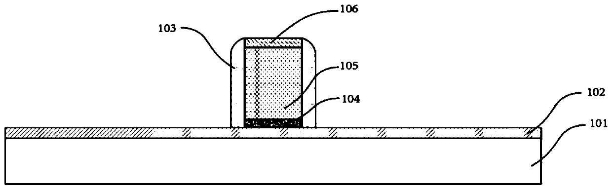
[0062] According to step S1, firstly, a semiconductor layer 102 is deposited on the substrate 101, and a gate structure having sidewalls 103 and gate electrodes is formed on the semiconductor layer 102, wherein the sidewalls 103 are located on both sides of the gate electrode. The substrate 101 mainly plays a supporting role, and can be hard insulating materials such as silicon oxide, silicon nitride, quartz, glass, aluminum oxide, etc., and high-temperature-resistant flexible insulating materials such as PET, PEN, polyimide, etc., as long as it is very flat and uni...
Embodiment 2
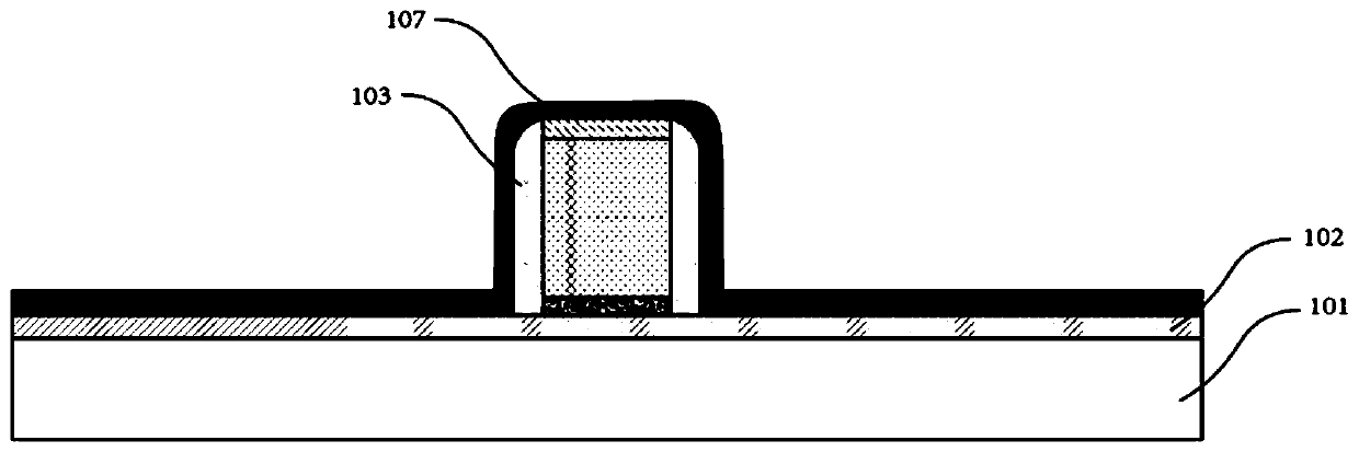
[0077] Figure 10 It shows the process steps of the non-doped thin film transistor prepared by the high-K metal gate-last gate process in the present invention, according to the following Figure 10 The steps shown and Figure 11-23 Another specific embodiment of the present invention is described in detail.
[0078] Follow step S1, such as Figure 11 As shown, a semiconductor layer 202 is deposited on a substrate 201, and a dummy gate structure with sidewalls 203 and dummy gates 204 is formed on the semiconductor layer 202, wherein the sidewalls 203 are located on both sides of the dummy gate 204, and the dummy gate structure is formed on the semiconductor layer 202. The material of the gate electrode 204 may be polysilicon or amorphous silicon, and a polysilicon dummy gate electrode is used in this embodiment. According to actual needs, one or more gate dielectric layers (not shown in the figure) are often grown on the semiconductor layer 202. The material of the gate die...
PUM
 Abstract
Description
Claims
Application Information
 - R&D Engineer
- R&D Manager
- IP Professional
- Industry Leading Data Capabilities
- Powerful AI technology
- Patent DNA Extraction
Browse by: Latest US Patents, China's latest patents, Technical Efficacy Thesaurus, Application Domain, Technology Topic, Popular Technical Reports.
© 2024 PatSnap. All rights reserved.Legal|Privacy policy|Modern Slavery Act Transparency Statement|Sitemap|About US| Contact US: help@patsnap.com