Single crystal single domain piezoelectric film and preparation method thereof

A technology of piezoelectric thin film and single crystal thin film, applied in the direction of piezoelectric/electrostrictive/magnetostrictive devices, circuits, electrical components, etc. High cost and other issues, to achieve the effect of no drop in electromechanical coupling coefficient, stable piezoelectric performance, and low cost

Active Publication Date: 2019-12-17
JINAN JINGZHENG ELECTRONICS
View PDF3 Cites 5 Cited by
  • Summary
  • Abstract
  • Description
  • Claims
  • Application Information

AI Technical Summary

Problems solved by technology

However, this method is not suitable for the production of thin-film substrate materials. The reason is that electrodes need to be applied on both sides of each piece. The cost of mass production and application is high, and the process is cumbersome, so mass production cannot be realized; in addition, due to the silicon substrate and the The thermal expansion coefficients of lithium niobate and lithium tantalate are quite different, and the film is easily broken when heated above the Curie temperature

Method used


Image

  • Single crystal single domain piezoelectric film and preparation method thereof
  • Single crystal single domain piezoelectric film and preparation method thereof

Examples


preparation example Construction

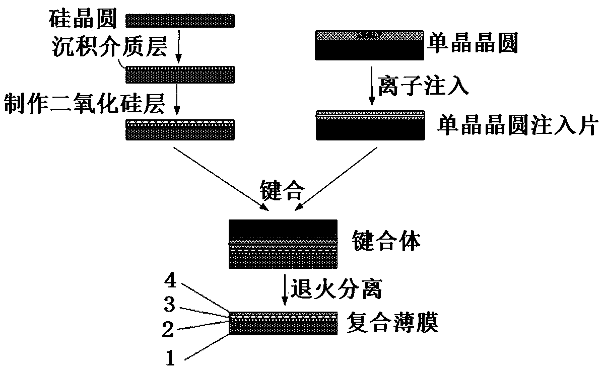
[0038] The present invention also includes a method for preparing a single crystal single domain piezoelectric film, comprising the following steps:

[0039] Preparation of composite films;

[0040] Put the composite film in an annealing furnace at 450-590°C and keep it warm for 5-30 minutes; or, put the composite film in an annealing furnace to heat up and anneal, and use an ion gun to spray charged ions onto the surface of the composite film during the heating process to obtain a single crystal Monodomain piezoelectric films.

[0041] The composite thin film of the present invention can be any existing single crystal thin film, such as lithium niobate thin film, lithium tantalate thin film, etc., all of which can be obtained by the method described in the present invention.

[0042] Preferably, the composite film is put into an annealing furnace during the temperature-raising annealing process, and the temperature is raised to 450-590° C. at a rate of 2-15° C. / minute.

[0...

Embodiment 1

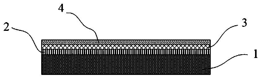
[0057] A single-crystal single-domain piezoelectric film, which sequentially includes a single-crystal film layer, a silicon dioxide layer, a dielectric layer, and a single-crystal silicon layer; wherein the material of the single-crystal film layer is single-crystal lithium niobate, and the ferroelectric domain is a single-domain , The piezoelectric coefficient is 98% to 100% of the bulk material; the dielectric layer is the damaged layer of single crystal silicon.

[0058] The single crystal lithium niobate in the material of the single crystal thin film layer can be replaced by single crystal lithium tantalate; the damaged layer of single crystal silicon in the dielectric layer can be replaced by amorphous silicon or polycrystalline silicon.

Embodiment 2

[0060] A single-crystal single-domain piezoelectric film, which sequentially includes a single-crystal film layer, a silicon dioxide layer, a dielectric layer, and a single-crystal silicon layer; wherein the material of the single-crystal film layer is single-crystal lithium niobate, and the ferroelectric domain is a single-domain , The piezoelectric coefficient is 98% to 100% of the bulk material; the dielectric layer is the damaged layer of single crystal silicon.

[0061] The thickness of the single crystal thin film layer is 100nm, the thickness of the silicon dioxide layer is 100nm; the thickness of the dielectric layer is 100nm, and the thickness of the single crystal silicon is 200μm.


PUM


Abstract

The invention discloses a single crystal single domain piezoelectric film and a preparation method thereof. The single crystal single domain piezoelectric film sequentially comprises a single crystalfilm layer, a silicon dioxide layer, a dielectric layer and a single crystal silicon layer. The material of the single crystal film layer is single crystal lithium niobate or single crystal lithium tantalate. The dielectric layer is a damaged layer of monocrystalline silicon, amorphous silicon or polycrystalline silicon. The piezoelectric coefficient of the single crystal single domain piezoelectric film is 98-100% of that of the body material, while the piezoelectric coefficient in the prior art is 10-90% of that of the body material. The single domain single crystal film has stable piezoelectric performance in use, the electromechanical coupling coefficient does not decrease, the device bandwidth is wide, the loss is low and the consistency is good. The preparation method of the single crystal single domain piezoelectric film has low cost, low energy consumption and high efficiency and is suitable for industrial production and has high yield. The silicon dioxide layer of tens of nanometers in the obtained film can achieve the effects of controllable thickness, small thickness deviation, flat surface and good uniformity, thus the obtained device has good consistency.

Description

technical field [0001] The invention relates to the technical field of single crystal thin films, in particular to a single crystal single domain piezoelectric thin film and a preparation method thereof. Background technique [0002] Lithium niobate and lithium tantalate single crystal thin films are widely used in acoustic wave devices, optical signal processing, information storage, and electronic devices. Using them as basic materials can produce large-bandwidth, low-temperature drift, low-loss acoustic wave devices and High-frequency, high-bandwidth, high-capacity optoelectronic devices and integrated optical circuit chips. [0003] Although the lithium niobate and lithium tantalate single crystal thin films prepared by ion implantation and stripping are single crystal in crystal structure, part of the polarization domain is reversed, so this will make the prepared piezoelectric substrate more domain single crystal. However, multi-domain single crystals will reduce the...

Claims


Application Information

Patent Timeline
Patent Type & Authority Applications(China)
IPC IPC(8): H01L41/187H01L41/253H01L41/257
CPCH10N30/8542H10N30/04H10N30/045
Inventor 李真宇胡文张秀全罗具廷杨超
Owner JINAN JINGZHENG ELECTRONICS
Why Eureka
Try Eureka