Closed planar three-electrode spark switch and preparation method thereof
A spark switch, three-electrode technology, applied in the direction of spark plugs, spark gaps, spark gap components, etc., can solve the problem of unstable self-breakdown performance and conduction performance of the switch, influence of circuits around the spark, and poor performance of high overload resistance Better and other problems, to achieve the effect of shortening the processing cycle, low price, strong ablation resistance
- Summary
- Abstract
- Description
- Claims
- Application Information
AI Technical Summary
Problems solved by technology
Method used
Image
Examples
preparation example Construction
[0035] The preparation process of the closed planar three-electrode switch is as follows:
[0036] The process includes concrete steps as follows:
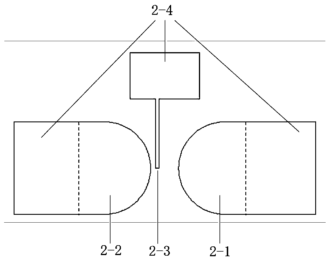
[0037] The first step is to clean the bottom PCB (1), and use the methods of exposure, development, and etching to coat copper on the upper surface of the bottom PCB 1 to obtain the circuit pattern corresponding to the switch, including the anode 2-1 of the switch. , cathode 2-2, trigger electrode 2-3 and pad 2-4 connected thereto.
[0038] In the second step, the pads 2-4 on the circuit layer are treated with chemical nickel gold or tin spraying to ensure the solderability and flatness of the pads; the anode 2-1 and cathode 2-2 on the circuit layer are Carry out immersion gold or gold plating and other process treatments with the trigger electrodes 2-3 to prevent the electrodes from being oxidized.
[0039] The fourth step is to use laser or mechanical cutting to open a window on the area corresponding to the pad and electrode ...
Embodiment 1
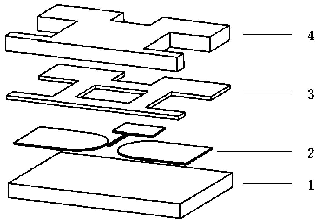
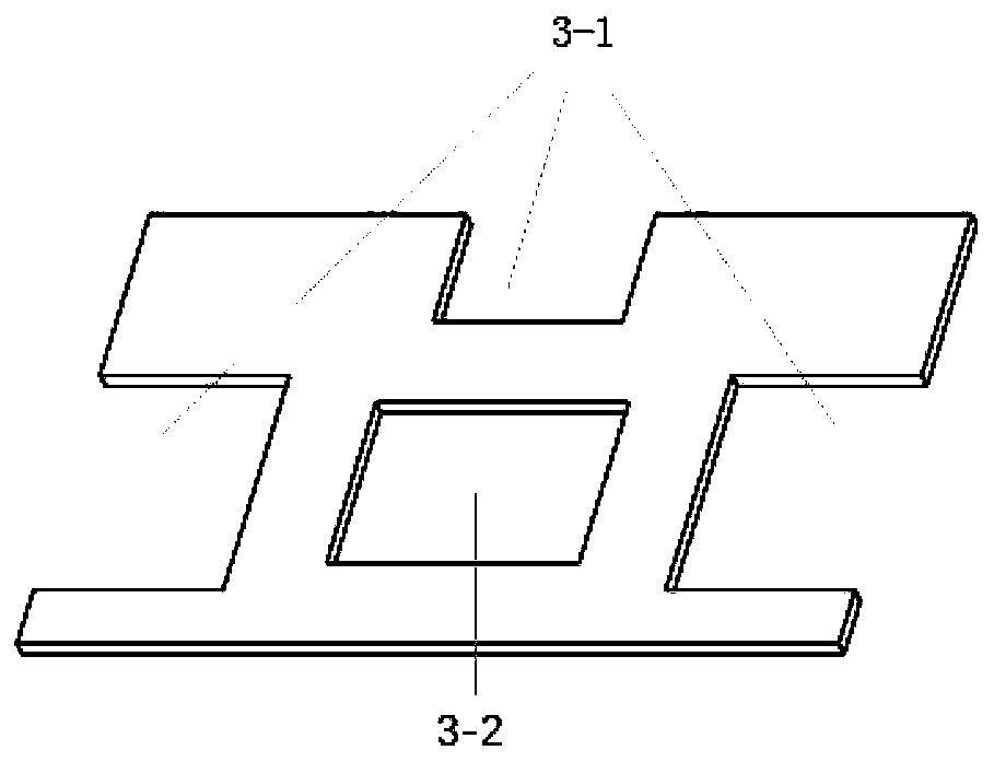
[0044]In this implementation case, a closed planar three-electrode spark switch based on printed circuit board technology is designed. According to the printed circuit board process and its processing steps, the switch can be divided into four parts: the bottom PCB board 1 , the circuit layer 2 , the PP layer 3 and the top PCB board 4 . The thickness of the bottom PCB board 1 is 1mm, and the material is FR-4, which is used as the carrier of the circuit layer in the whole switch. The circuit layer 2 directly etches the copper on the upper surface of the bottom PCB 1 by printing ink, developing, etching, and stripping the film to obtain the pattern corresponding to the switch. The thickness of the circuit layer is 35 μm. The circuit layer includes three electrodes of the planar three-electrode switch, that is, the anode 2-1, the cathode 2-2 and the trigger electrode 2-3 and the three pads 2-4 connected thereto; the anode and the cathode are semicircular electrodes, and the elect...
PUM
| Property | Measurement | Unit |
|---|---|---|
| Thickness | aaaaa | aaaaa |
| Thickness | aaaaa | aaaaa |
| Thickness | aaaaa | aaaaa |
Abstract
Description
Claims
Application Information


