Memristor with double resistance change layer and preparation method

A technology of resistive variable layer and memristor, which is applied in the direction of electrical components, etc., can solve the problems of uneven distribution of high and low resistance states, weak photoferroelectric response, and poor durability, and achieve good durability, long retention time, and preparation The effect of simple method

Pending Publication Date: 2020-01-10
HUBEI UNIV
View PDF3 Cites 5 Cited by
  • Summary
  • Abstract
  • Description
  • Claims
  • Application Information

AI Technical Summary

Problems solved by technology

[0004] The structure of the memristor is generally a sandwich structure of metal / insulating layer / metal, in which the metal is the upper and lower electrodes, and the insulating layer is the resistance transition layer; the material of the insulating layer has a great influence on the performance of the resistive variable memory. In order to obtain better performance, Many materials are used in resistive variable memory, such as multi-element perovskite oxides, binary metal oxides, chalcogenide solid electrolytes, nitrides, amorphous silicon, amorphous carbon, etc. Traditional single-layer resistive variable layer devices perform Stable bipolar resistive switching performance and consistency, but there are still problems of small switch ratio and poor durability
[0005] Ferroelectric materials show superior characteristics in the application of memristors, but they still have limitations. For example, Ayan Sarkar in Multifunctional BiFeO 3 / TiO 2 nano-heterostructure: Photo-ferroelectricity, rectifyingtransport, and nonvolatile resistive switchingproperty reported that as the applied voltage increases, the photoferroelectric response of BiFeO3 nanostructures becomes weaker; J.M.Luo in Resistive switching and Schottky diode-like behaviors in Pt / BiFeO 3 / ITOdevices reports that there are uneven distribution of high and low resistance states

Method used


Image

  • Memristor with double resistance change layer and preparation method
  • Memristor with double resistance change layer and preparation method
  • Memristor with double resistance change layer and preparation method

Examples


Embodiment 1

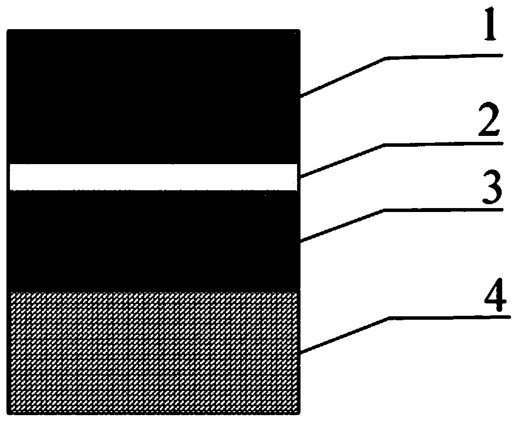
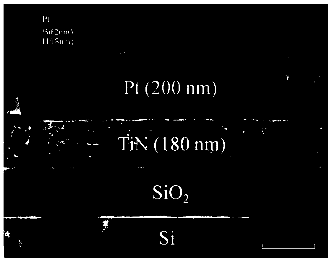
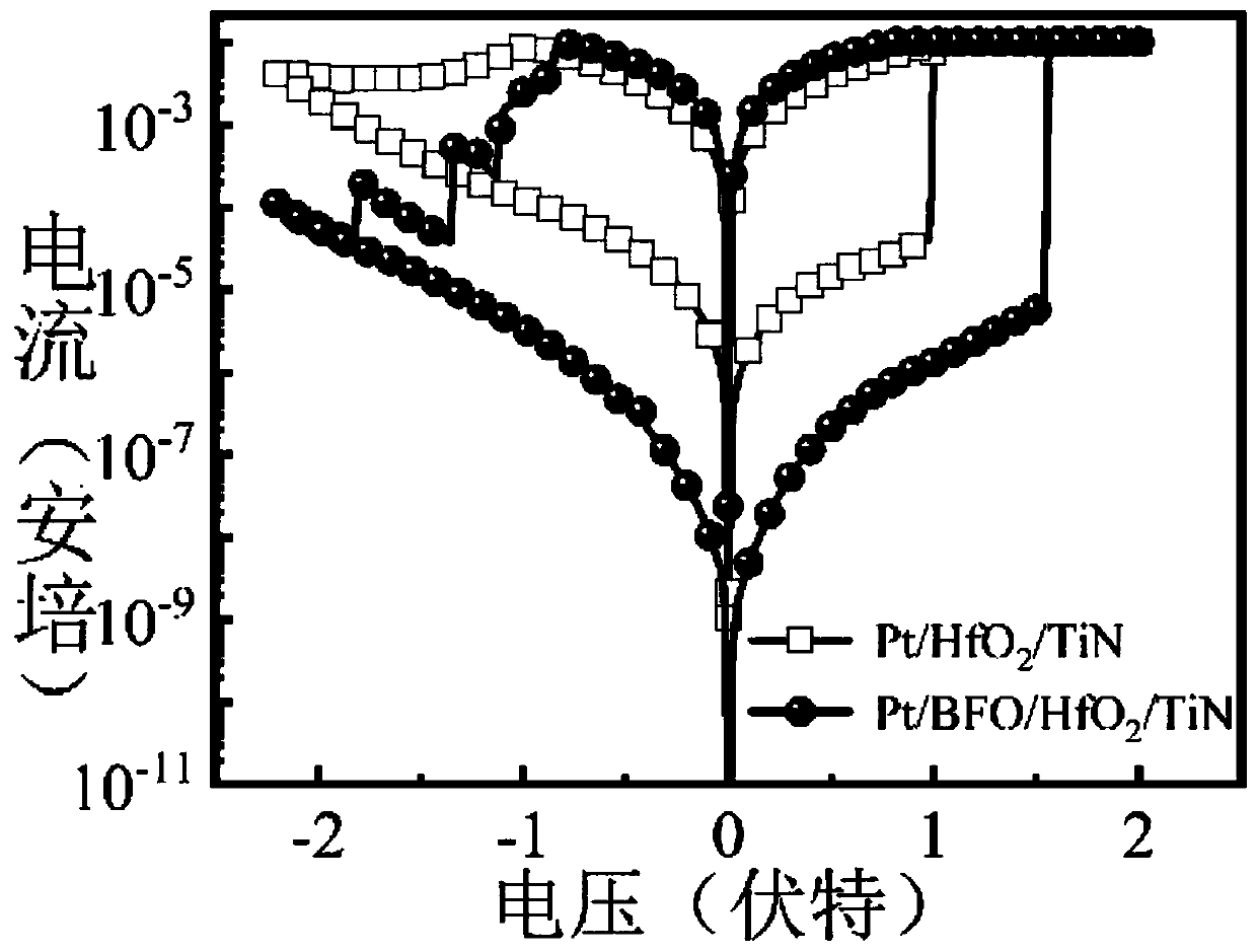
[0038] A memristor, which is mainly composed of a silicon oxide substrate, a bottom electrode, a first resistive layer, a second resistive layer and a top electrode, wherein the material of the bottom electrode is titanium nitride (TiN) with a thickness of 200nm, The material of the first resistive layer is hafnium oxide (HfO 2 ), the material of the second resistive switch layer is bismuth ferrite (BFO) with a thickness of 8nm and 2nm respectively, and the material of the top electrode is platinum (Pt) with a thickness of 200nm.

[0039] Step 1, cleaning the silicon oxide wafer

[0040] Place the silicon oxide wafer in an ultrasonic instrument, and use acetone, absolute ethanol, and deionized water to sonicate for 15 minutes respectively;

[0041] Step 2, prepare the bottom electrode

[0042] Prepare a layer of titanium nitride bottom electrode on the silicon substrate by magnetron sputtering method, and the vacuum degree of magnetron sputtering is less than 10 - 4 Pa, th...

Embodiment 2

[0052] A memristor, which is mainly composed of a silicon oxide substrate, a bottom electrode, a first resistive layer, a second resistive layer and a top electrode, wherein the material of the bottom electrode is titanium nitride (TiN) with a thickness of 200nm, The material of the first resistive layer is hafnium oxide (HfO 2 ), the material of the second resistive switch layer is bismuth ferrite (BFO) with a thickness of 8nm and 1nm respectively, and the material of the top electrode is platinum (Pt) with a thickness of 200nm.

[0053] Step 1, cleaning the silicon oxide wafer

[0054] Place the silicon oxide wafer in an ultrasonic instrument, and use acetone, absolute ethanol, and deionized water to sonicate for 15 minutes respectively;

[0055] Step 2, prepare the bottom electrode

[0056] Prepare a layer of titanium nitride bottom electrode on the silicon substrate by magnetron sputtering method, and the vacuum degree of magnetron sputtering is less than 10 - 4 Pa, th...

Embodiment 3

[0066] A memristor, which is mainly composed of a silicon oxide substrate, a bottom electrode, a first resistive layer, a second resistive layer and a top electrode, wherein the material of the bottom electrode is titanium nitride (TiN) with a thickness of 200nm, The material of the first resistive layer is hafnium oxide (HfO 2 ), the material of the second resistive switch layer is bismuth ferrite (BFO) with a thickness of 8nm and 9nm respectively, and the material of the top electrode is platinum (Pt) with a thickness of 200nm.

[0067] Step 1, cleaning the silicon oxide wafer

[0068] Place the silicon oxide wafer in an ultrasonic instrument, and use acetone, absolute ethanol, and deionized water to sonicate for 15 minutes respectively;

[0069] Step 2, prepare the bottom electrode

[0070] Prepare a layer of titanium nitride bottom electrode on the silicon substrate by magnetron sputtering method, and the vacuum degree of magnetron sputtering is less than 10 - 4 Pa, th...


PUM

PropertyMeasurementUnit
thicknessaaaaaaaaaa
thicknessaaaaaaaaaa
thicknessaaaaaaaaaa

Abstract

The invention provides a memristor with double resistance change layer and a preparation method. The memristor with double resistance change layer comprises a bottom electrode, a first resistance change layer, a second resistance change layer and a top electrode which are stacked in sequence, wherein the first resistance change layer is prepared from one or more of multi-element perovskite oxide,binary metal oxide, chalcogenide solid electrolyte or nitride; and the second resistance change layer is prepared from a ferroelectric material. The memristor has the beneficial effects that (1) the preparation method is simple and easy to operate; (2) the memristor has the advantages of large resistance change window, good device durability, long retention time and the like after being inserted into the resistance change layer prepared from the ferroelectric material, and obtains a multi-stage storage function; (3) the resistance can be continuously regulated and controlled when voltage stimulation is applied, and a biological synapse bionic function is achieved; and (4) time sequence dependence synaptic plasticity learning rules in the biological synapses can be simulated, and an autonomous learning function is achieved.

Description

technical field [0001] The invention belongs to the field of information processing materials, and in particular relates to a double resistance variable layer memristor and a preparation method. Background technique [0002] With the advent of the era of big data, the explosive growth of a large amount of information requires super-large-capacity storage devices and super-efficient information processing systems. These requirements promote the rapid development of the information technology industry. Traditional computer systems based on the von Neumann system Due to its shortcomings such as low efficiency and high energy consumption, it has become increasingly difficult to meet the requirements, and a new computing system is in urgent need of construction. Neuromorphic computing systems have the characteristics of high efficiency, good fault tolerance, and self-adaptation, and have been widely studied as potential technologies to replace traditional digital computing system...

Claims


Application Information

Patent Timeline
Patent Type & Authority Applications(China)
IPC IPC(8): H01L45/00
CPCH10N70/881H10N70/8836H10N70/026
Inventor 叶葱刘磊柯善武刘炎欣
Owner HUBEI UNIV
Why Eureka
Try Eureka