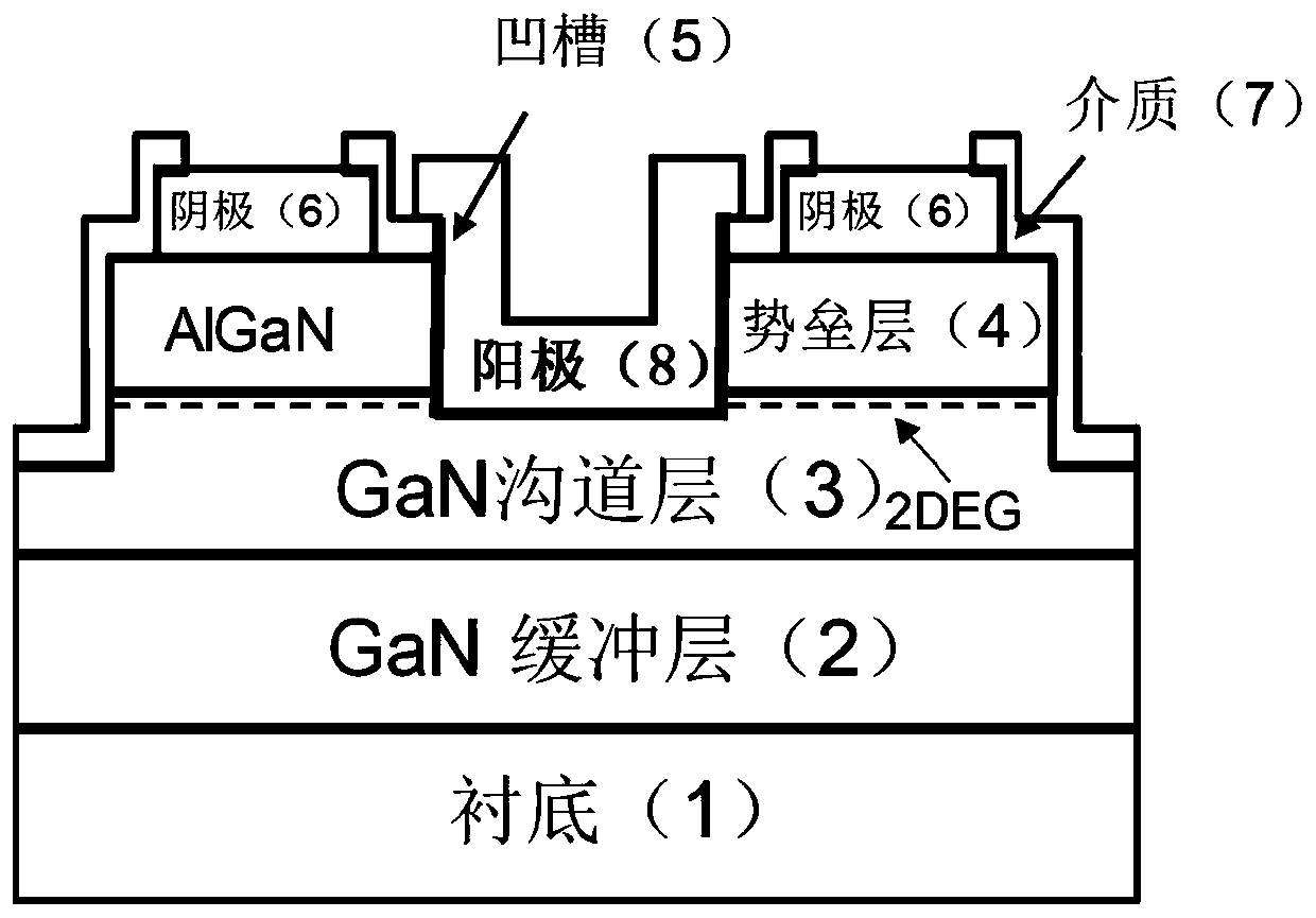
Low-turn-on-voltage GaN microwave diode based on low-work-function anode metal and preparation method thereof
A technology with low turn-on voltage and low work function, which is applied in the field of microelectronics, can solve the problems of high turn-on voltage of microwave diodes, large difference in metal work function, high Schottky barrier, etc., to achieve reduced turn-on voltage, small work function difference, The effect of reducing the contact barrier
- Summary
- Abstract
- Description
- Claims
- Application Information
AI Technical Summary
Problems solved by technology
Method used
Image
Examples
Embodiment 1
[0041] Example 1, a low turn-on voltage GaN microwave diode with a SiN layer thickness of 200nm, an anode groove etched to 5nm below the AlGaN / GaN interface, and an anode metal of Mo / Au with a thickness of 30 / 200nm was fabricated.
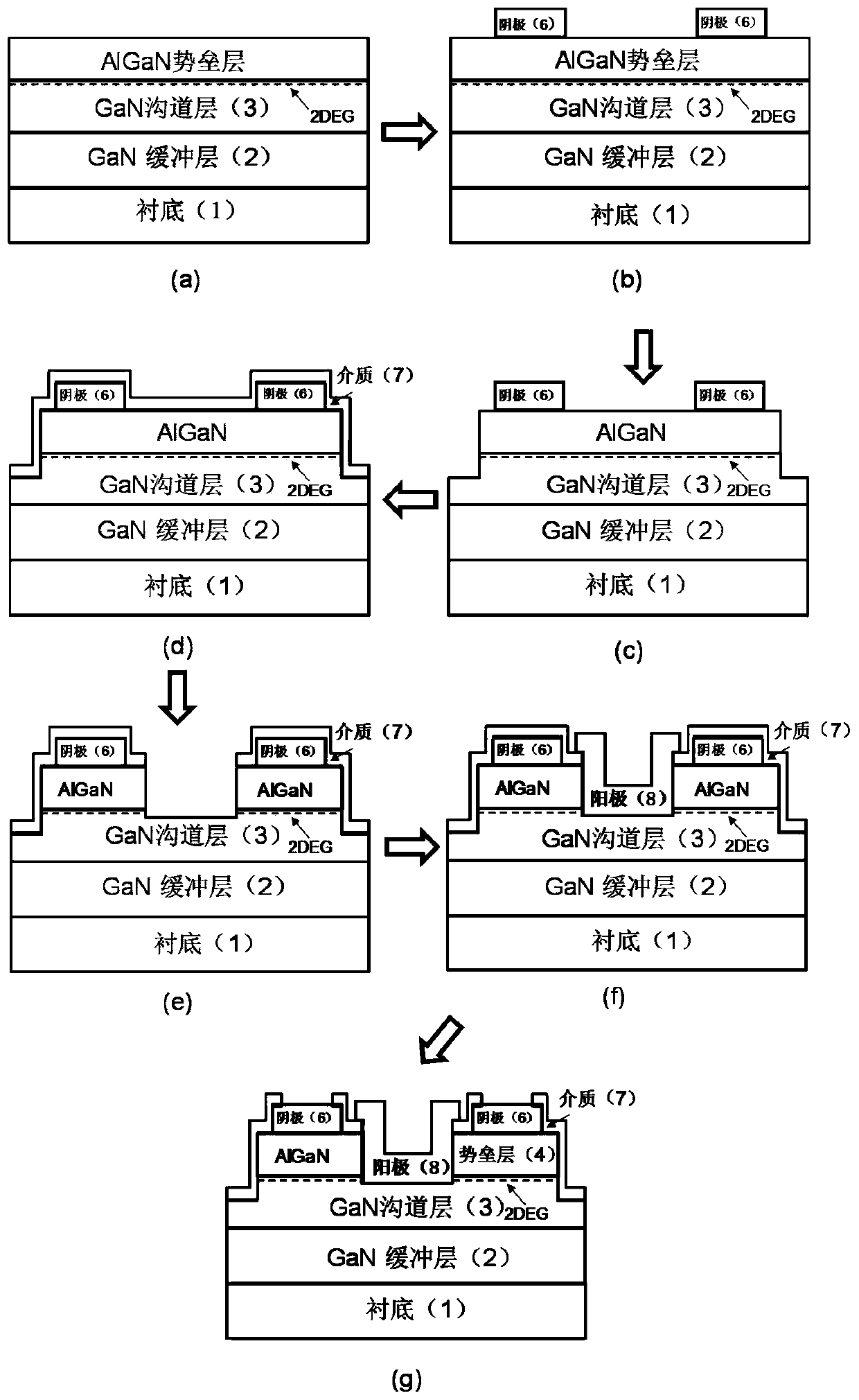
[0042] Step 1, epitaxial wafer cleaning, such as figure 2 (a).
[0043] The epitaxial wafer with AlGaN / GaN structure was soaked in HF acid solution or HCl acid solution for 30s, then placed in acetone solution, absolute ethanol solution and deionized water for 5min ultrasonic cleaning each, and then blown dry with nitrogen.
[0044] Step 2, make GaN microwave diode cathode, such as figure 2 (b).
[0045] 2a) On a clean epitaxial wafer, perform uniform coating, baking, photolithography and development of the cathode area of the device in sequence, and use electron beam evaporation equipment to deposit Ti / Al / Ni / Au metal stacks on the epitaxial wafer with a thickness of 22 / 140 / 55 / 45nm;
[0046] 2b) Soak the epitaxial wafer deposited with Ti / A...
Embodiment 2
[0062] Example 2, making a low turn-on voltage GaN microwave diode with a SiN layer thickness of 300nm, an anode groove etched to 10nm below the AlGaN / GaN interface, and an anode metal of W / Au with a thickness of 40 / 200nm:
[0063] Step 1, epitaxial wafer cleaning, such as figure 2 (a).
[0064] The specific implementation of this step is the same as step 1 of Embodiment 1.
[0065] Step 2, making GaN microwave diode cathode, such as figure 2 (b).
[0066] The specific implementation of this step is the same as that of step 2 in Embodiment 1.
[0067] Step 3, making countertop isolation, such as figure 2 (c).
[0068] The specific implementation of this step is the same as that of step 3 in Embodiment 1.
[0069] Step 4, use plasma-enhanced chemical vapor deposition equipment to deposit a SiN dielectric with a thickness of 300nm on the epitaxial wafer after mesa isolation, such as figure 2 (d).
[0070] Step five, make the anode groove, such as figure 2 (e).
[...
Embodiment 3
[0078] Embodiment 3, making SiO 2 A low turn-on voltage GaN microwave diode with a layer thickness of 200nm, an anode groove etched to 15nm below the AlGaN / GaN interface, and an anode metal of Mo with a thickness of 200nm:
[0079] Step A, epitaxial wafer cleaning, such as figure 2 (a).
[0080] The specific implementation of this step is the same as step 1 of Embodiment 1.
[0081] Step B, making GaN microwave diode cathode, such as figure 2 (b).
[0082] The specific implementation of this step is the same as that of step 2 in Embodiment 1.
[0083] Step C, making countertop isolation, such as figure 2 (c).
[0084] The specific implementation of this step is the same as that of step 3 in Embodiment 1.
[0085] Step D, depositing SiN dielectric. like figure 2 (d).
[0086] Deposit SiO with a thickness of 200nm on the mesa-isolated epitaxial wafer using plasma-enhanced chemical vapor deposition equipment 2 medium.
[0087] Step E, make the anode groove, such a...
PUM
| Property | Measurement | Unit |
|---|---|---|
| Thickness | aaaaa | aaaaa |
| Thickness | aaaaa | aaaaa |
| Thickness | aaaaa | aaaaa |
Abstract
Description
Claims
Application Information

