

Preparation method for single-layer MoS2-WS2 transverse heterojunction
A mos2-ws2, heterojunction technology, applied in semiconductor/solid-state device manufacturing, electrical components, circuits, etc., can solve the problems of strict experimental conditions, influence of interface amorphization, difficulty in obtaining high-quality samples, etc., and achieve controllable Strong, simple effect
- Summary
- Abstract
- Description
- Claims
- Application Information
AI Technical Summary
Problems solved by technology
Method used
Image

Examples
Embodiment 1
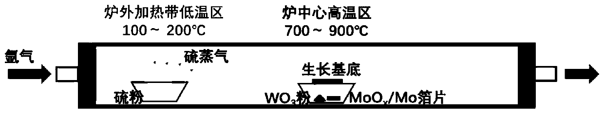
[0031] A single-layer MoS 2 -WS 2 The preparation method of the lateral heterojunction is carried out according to the following steps:
[0032] In this experiment, 400 μm thick SiO 2 / Si (where SiO 2 300nm) as the growth substrate, first cut a 4-inch silicon wafer into a 1cm×1cm square substrate; secondly, ultrasonically clean the cut silicon wafer for 20 minutes according to the order of acetone, alcohol, and deionized water, Set the power to 70W to clean the surface.
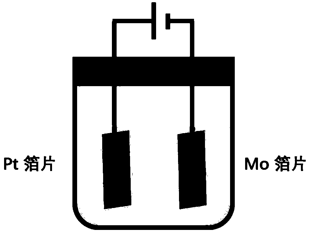
[0033] Preparation of the molybdenum source precursor: configuration of the electrolyte, use an electronic balance to weigh oxalic acid and sodium fluoride, respectively, 9.45g and 0.21g, put them into a beaker and stir to dissolve, add deionized water to dissolve and pour into a volumetric flask, Set the volume to 500ml; cut the molybdenum foil with a purity of 99.99% to a size of 1x 1cm; electrochemical oxidation, using an electrochemical workstation to oxidize the molybdenum foil to prepare MoO x / Mo f...
PUM
 Abstract
Description
Claims
Application Information