

P-GaN ohmic contact electrode and preparation method and application thereof
A technology of ohmic contact electrodes and p-gan, which is applied in the manufacture of circuits, electrical components, semiconductors/solid-state devices, etc. It can solve the problems that it is difficult to increase the hole concentration of p-GaN materials, and it is difficult to achieve ohmic contact than contact resistivity. , to achieve the effect of improving electrical properties and reducing specific contact resistivity
- Summary
- Abstract
- Description
- Claims
- Application Information
AI Technical Summary
Problems solved by technology
Method used
Image

Examples
preparation example Construction
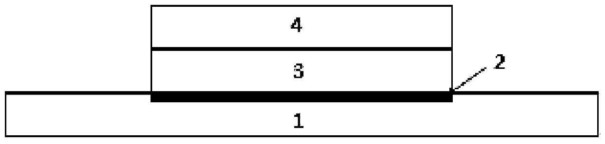
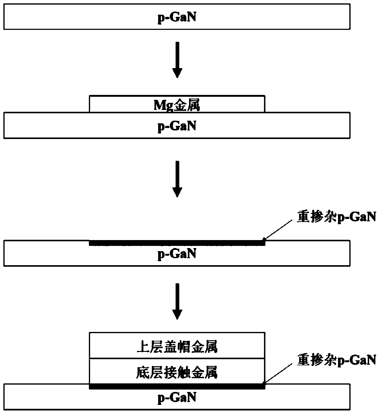
[0039] see figure 2 , a method for preparing a p-GaN ohmic contact electrode according to an embodiment of the present invention, comprising the following steps:
[0040] 1) Clean the p-GaN material by standard cleaning organic and inorganic cleaning process. After cleaning, N 2 blow dry;
[0041] 2) Depositing Mg metal on the p-GaN material cleaned in step 1), and performing high-temperature annealing treatment to obtain a sample after high-temperature annealing treatment;
[0042] 3) After the high-temperature annealing sample is cleaned by HCl and HF, the residual Mg metal on the surface is removed, and a highly doped p-GaN region is formed under the Mg metal region, that is, a p-GaN heavily doped layer;
[0043] 4) In the highly doped p-GaN region, deposit the bottom contact metal and the upper cap metal in sequence, and perform annealing treatment to form a good ohmic contact.
[0044] Preferably, the deposition method of Mg metal in step 2) is thermal evaporation, elec...
Embodiment 1
[0049] A method for preparing a p-GaN ohmic contact electrode according to an embodiment of the present invention includes the following steps:
[0050] 1) Spin-coat a layer of AZ5214 photoresist on the surface of the p-GaN material after cleaning, bake the p-GaN sample with the spin-coated photoresist at 95°C for 90 seconds, and use the designed mask plate for ultraviolet lithography Expose for 4s, develop for 30s to remove the exposed photoresist, leaving a window for depositing Mg metal;
[0051] 2) Place the p-GaN sample after photolithography in the electron beam evaporation equipment, and pump the background vacuum to 5×10 -4 After Pa, 10 nm of Mg metal was deposited on the surface of the sample, and the deposition method was thermal evaporation. Take out the p-GaN sample that has been deposited, soak it in N-methylpyrrolidone (NMP) solution, and put it in a water bath at 120°C for 5 minutes, and then ultrasonically peel off the metal outside the exposed area to obtain ...
Embodiment 2
[0058] A method for preparing a p-GaN ohmic contact electrode according to an embodiment of the present invention includes the following steps:
[0059] 1) Place the cleaned p-GaN material in plasma-enhanced vapor-phase chemical deposition (PECVD), and deposit a layer of 20nm SiO on its surface 2 ;
[0060] 2) Containing SiO 2 Spin-coat a layer of AZ5214 photoresist on the surface of the p-GaN material, bake the p-GaN sample with the spin-coated photoresist at 95°C for 90 seconds, use the designed mask to expose to ultraviolet lithography for 4s, and develop 30s to remove the exposed photoresist;
[0061] 3) Harden the photolithographic sample on a hot plate at 120°C for 120 seconds, soak in 5:1 BOE buffer for 30 seconds to remove the exposed SiO 2 , open the Mg metal deposition window;
[0062] 4) The p-GaN sample containing the Mg metal window was placed in the sputtering process, and the background vacuum was evacuated to 5×10 -4 After Pa, deposit 1 nm of Mg metal on t...
PUM
| Property | Measurement | Unit |
|---|---|---|
| thickness | aaaaa | aaaaa |
| thickness | aaaaa | aaaaa |
| thickness | aaaaa | aaaaa |
Abstract
Description
Claims
Application Information