A low-defect high-transmittance diamond growth method and system

A technology with high light transmittance and growth method, applied in the field of diamond manufacturing, can solve the problems of reducing defect density, reducing growth rate, increasing plasma density, etc., achieving low surface defect density, uniform distribution of growth steps, and transparent appearance. Effect

Active Publication Date: 2022-02-11
CHANGSHA ADVANCED MATERIALS IND RES INST CO LTD
View PDF7 Cites 0 Cited by
  • Summary
  • Abstract
  • Description
  • Claims
  • Application Information

AI Technical Summary

Problems solved by technology

By doping N2, especially 4ppm N 2 When , the surface etching pit will grow rapidly within 1.5h. By carefully selecting the initial growth process conditions, the H 2 / O 2 Etching pits to obtain a smooth film, but this scheme introduces nitrogen impurities, and the initial growth process conditions are harsh, even if small process parameters such as temperature, carbon content, H 2 / O 2 Etching time, etc., that will re-grow defects such as hillocks
Y. Mokuno et al. improved the substrate platform, changing the shape of the planar open structure into a closed structure shape. The change of the seed crystal arrangement can effectively increase the plasma density on the seed crystal surface, and make the seed crystal epitaxy The surface morphology is smooth and the defect density is significantly reduced, but the growth of polycrystalline edge is still not effectively inhibited
[0005] The patent document whose invention number is 02826062.7 discloses a device and a method for producing diamond, and the CH 4 / H 2 / N 2 In the case of , while adding a certain proportion of O 2 , can reduce the growth temperature, improve the growth quality, but significantly reduce the growth rate

Method used


Image

  • A low-defect high-transmittance diamond growth method and system
  • A low-defect high-transmittance diamond growth method and system

Examples


Embodiment Construction

[0037] In order to make the object, technical solution and effect of the present invention more clear and definite, the present invention will be further described in detail below with reference to the accompanying drawings and examples. It should be understood that the specific embodiments described here are only used to explain the present invention, not to limit the present invention.

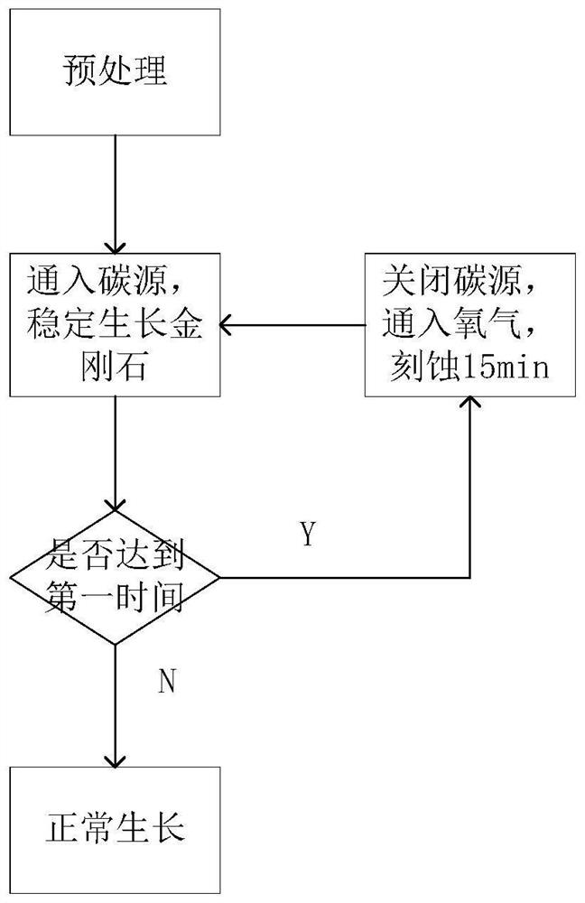
[0038] Please also refer to Figure 1-Figure 2 , the present invention provides a method for growing diamond with low defect and high light transmittance, comprising the steps of:

[0039] Oxygen is introduced at the first stage: the surface of the seed crystal is pretreated and placed in the growth chamber, and then a certain power of microwave is passed through, and hydrogen and oxygen are passed through to etch the surface of the seed crystal for 15-60 minutes; then, the oxygen is stopped, and the After entering a certain amount of argon, pass through the carbon source to generate carbon...


PUM


Abstract

The invention relates to a diamond growth method and system with low defects and high light transmittance. A diamond growth method with low defects and high light transmittance, comprising the steps of: feeding oxygen in stages: pretreating the surface of the seed crystal and putting it into a growth chamber, feeding microwaves with a certain power, and then feeding hydrogen and oxygen to the seed crystal Etch the surface for 15‑60min; then, stop feeding oxygen, feed a certain amount of argon, feed carbon source to generate carbon ion clusters, and then grow diamond stably; stop feeding carbon source, feed oxygen every first time Etching for 10-30min; substrate table lifting: while the stable growth, real-time detection of the thickness data of diamond growth, according to the thickness data, the height of the substrate table is controlled, so that the diamond growth surface is always in the best growth position . The present invention provides a low-defect high-transmittance diamond growth method and system. The grown diamond has a layered structure, and the content of oxygen element is periodically distributed as the thickness of the diamond increases.

Description

technical field [0001] The invention relates to the field of diamond manufacturing, in particular to a diamond growth method and system with low defects and high light transmittance. Background technique [0002] High-quality diamond has a high band gap and a wide light transmission spectrum. At the same time, it has ultra-high hardness and thermal conductivity, excellent insulation, and excellent physical and chemical properties such as acid resistance, heat resistance, and radiation resistance. It can be used in precision machining. , Optical windows, gemstones, MEMS (Micro-Electro-Mechanical System, Micro-Electro-Mechanical System), chips and other fields. However, high-quality natural diamond reserves are limited, so people have developed a variety of synthetic diamond methods, such as high temperature and high pressure method, hot wire chemical vapor deposition method. Among them, the MPCVD (Microwave plasma chemical vapor deposition, microwave plasma chemical vapor de...

Claims


Application Information

Patent Timeline
Patent Type & Authority Patents(China)
IPC IPC(8): C23C16/27C23C16/52C30B29/04C30B25/16
CPCC23C16/27C23C16/52C30B29/04C30B25/16
Inventor 彭国令黄翀
Owner CHANGSHA ADVANCED MATERIALS IND RES INST CO LTD
Why Eureka
Try Eureka