Patterned nuclear-shell nanoparticle surface enhanced Raman spectroscopy (SERS) active substrate and preparation method
A core-shell structure and nanoparticle technology, applied in nanotechnology, nanotechnology, nanotechnology for sensing, etc., can solve the problems of small preparation area and low production capacity, and achieve high sensitivity, low cost, and high steps. Effect
- Summary
- Abstract
- Description
- Claims
- Application Information
AI Technical Summary
Problems solved by technology
Method used
Image
Examples
Embodiment 1
[0032] Regular triangle patterned Ni 50 @Au 50 A method for preparing a core-shell structure nanoparticle SERS active substrate, specifically comprising the following steps:
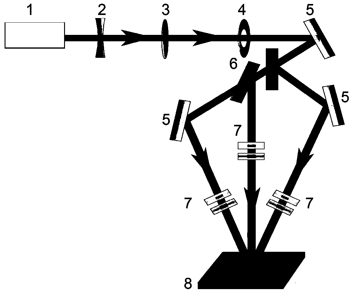
[0033] (1) Prepare a patterned substrate by laser interference: design the pattern as an equilateral triangle with a side length of 9 μm, build a laser interference system according to the expected pattern, and select a 1064nm Nd:YAG nanosecond laser (pulse width: 6ns, repetition frequency: 10Hz) to pass through the spectroscopic system Generate three beams of coherent light, adjust the energy density of the interference laser to 300mJ / cm 2 , the interfering light acts vertically on the surface of a single-sided polished 100-oriented single-crystal silicon wafer for 3 seconds, and ablates an equilateral triangle pattern with a side length of 9 μm. Wherever it works, it is the expected pattern.
[0034] figure 1 It is a three-beam laser interference ablation system, including 1064nm nanosecond laser 1...
Embodiment 2
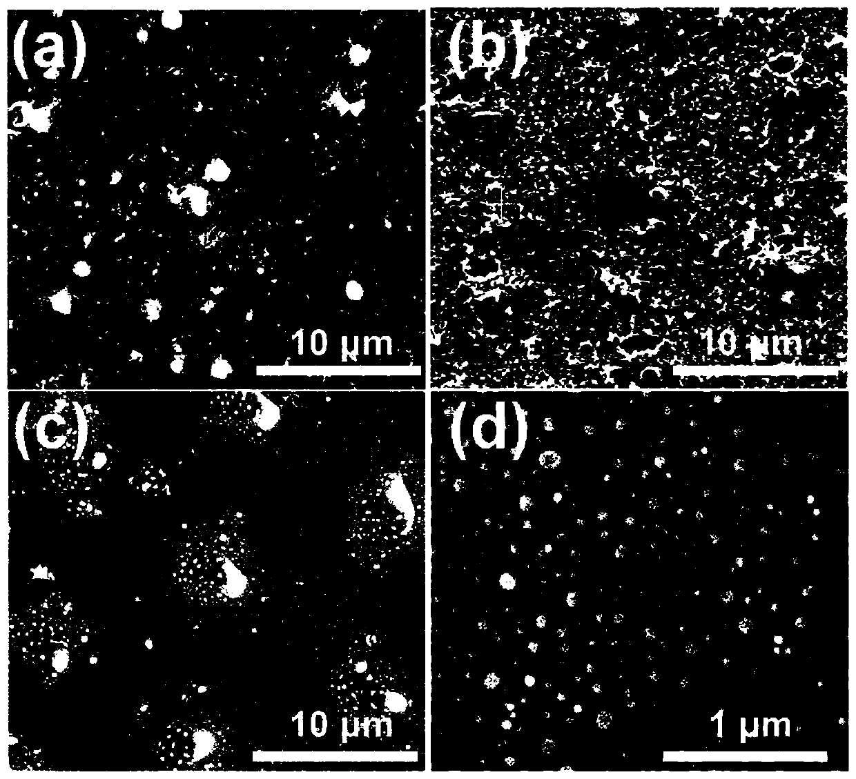
[0041] Adjust the gold-nickel component distribution ratio of the deposited double-layer metal film in embodiment 2: by the method for magnetron sputtering, be that 20nm Au film is deposited on the silicon substrate surface that step (1) obtains, other experimental parameters are all with embodiment 1, the obtained pure Au nanoparticles SEM image is as follows figure 2 shown. Test of SERS active substrate Raman spectroscopy: the Au nanoparticle substrate was placed at a concentration of 10 -6 In the solution of the R6G probe molecule of M, test condition is consistent with embodiment 1, and the Raman spectrum curve that obtains is as follows Figure 5 Shown in (1) in. According to Raman enhancement factor calculation formula EF=(I SERS / I NR )(C NR / C SERS ), where I SERS and I NR respectively in the selected 613cm -1 SERS intensity at Raman peak and normal Raman spectrum intensity, C SERS and C NR are the concentrations for SERS substrate and Si substrate, respect...
Embodiment 3
[0043] Regulate the gold-nickel composition ratio of deposition double-layer metal film among the embodiment 3: by the method for magnetron sputtering, be two kinds of metal films of 4nm Ni 16nm Au with thickness, successively deposit on the silicon substrate surface that step (1) obtains, other Experimental parameter is all consistent with embodiment 1, the obtained Ni 20 @Au 80 SEM images of core-shell nanoparticles figure 2 shown. Raman spectrum test of SERS active substrate: the Ni 20 @Au 80 The core-shell nanoparticle substrate was placed at a concentration of 10 -6 In the solution of the R6G probe molecule of M, test condition is consistent with embodiment 1, and the Raman spectrum curve that obtains is as follows Figure 5 In (2) shown. According to Raman enhancement factor calculation formula EF=(I SERS / I NR )(C NR / C SERS ), where I SERS and I NR respectively in the selected 613cm -1 SERS intensity at Raman peak and normal Raman spectrum intensity, C S...
PUM
| Property | Measurement | Unit |
|---|---|---|
| Thickness | aaaaa | aaaaa |
| Thickness | aaaaa | aaaaa |
| Thickness | aaaaa | aaaaa |
Abstract
Description
Claims
Application Information


