Silicon-based stress covariant substrate and preparation method thereof, gallium nitride LED and preparation method thereof

A technology of stress covariant layer and gallium nitride, which is applied in the direction of electrical components, circuits, semiconductor devices, etc., to achieve the effect of material size expansion, simple and practical process, and conducive to large-scale production and application promotion

Pending Publication Date: 2020-03-27
NANJING YOUTIAN METAL TECH +1
View PDF0 Cites 0 Cited by
  • Summary
  • Abstract
  • Description
  • Claims
  • Application Information

AI Technical Summary

Problems solved by technology

[0011] Purpose of the invention: The present invention aims to provide a silicon-based stress-compliant substrate that can overcome and alleviate the problem of large mismatch stress when using a Si single crystal substrate to realize high-quality preparation and growth of GaN materials and LED devices

Method used


Image

  • Silicon-based stress covariant substrate and preparation method thereof, gallium nitride LED and preparation method thereof
  • Silicon-based stress covariant substrate and preparation method thereof, gallium nitride LED and preparation method thereof

Examples


Embodiment 1

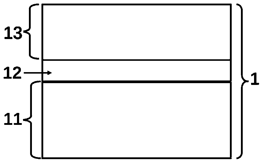
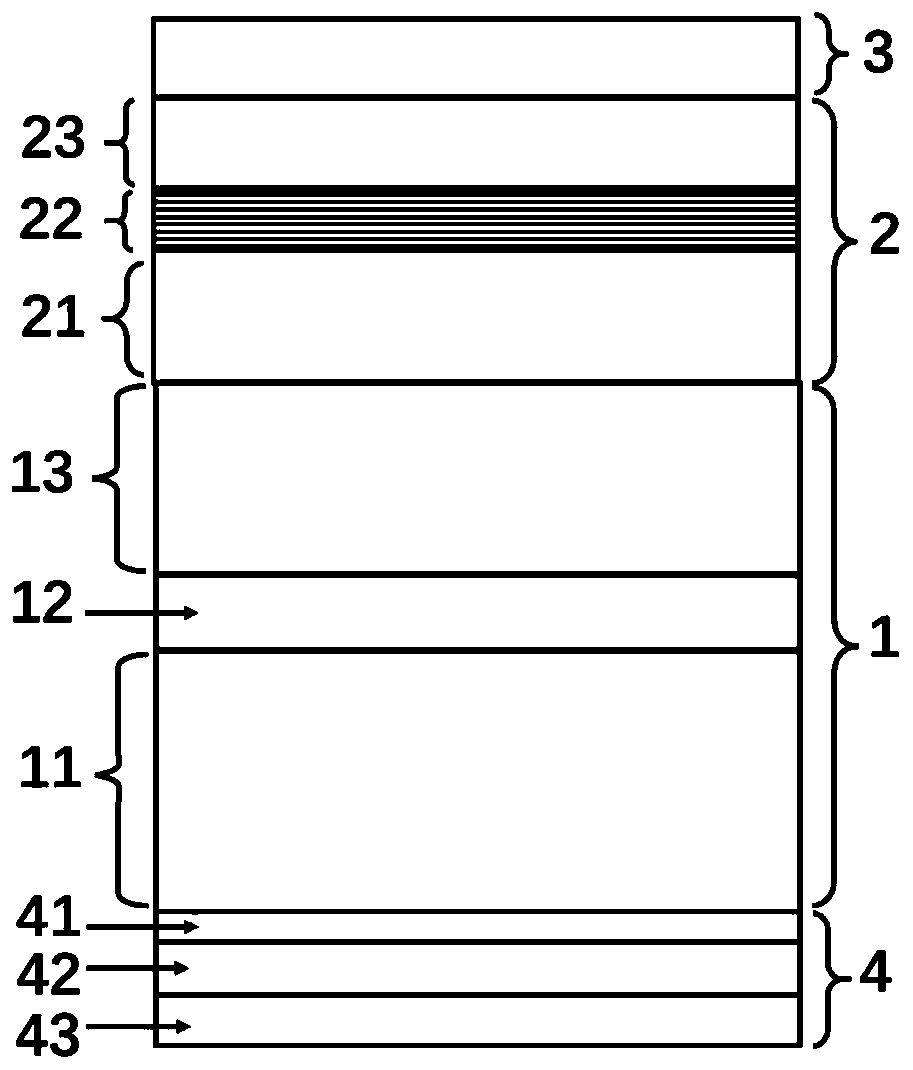
[0040] The invention discloses a silicon-based stress-covariant substrate, such as figure 1 As shown, it includes: a double-sided polished silicon (Si) single crystal substrate 11; a thin zirconium nitride (ZrN) conductive reflective stress covariant layer 12; a gallium nitride (GaN) single crystal thin film template layer 13.

[0041] The diameter of the double-sided polished silicon single crystal substrate includes but is not limited to 2 inches, 4 inches, 6 inches, 8 inches, 12 inches, and 18 inches.

[0042] The thin zirconium nitride conductive reflective stress-covariant layer 12 is formed on the double-sided polished silicon single crystal substrate 11, and is composed of a thin zirconium nitride (ZrN) film material with a thickness of 50nm to 350nm, which is used for transferring and coordinating the release of silicon (Si) Lattice mismatch stress, internal stress and thermal mismatch stress generated during the process of substantial cooling of gallium nitride (GaN) ...

Embodiment 2

[0058] Silicon (Si) single-crystal substrate 11, thin zirconium nitride (ZrN) conductive light-reflecting stress-conforming layer 12, thin gallium nitride (GaN) single-crystal thin-film template layer 13, and the silicon (Si)-based stress-conforming layer composed of the three Variable substrate 1, which can be used for single crystal thin films of gallium nitride, indium nitride, indium gallium nitride, indium aluminum gallium nitride, indium aluminum nitride, aluminum gallium nitride, aluminum nitride, zinc oxide, silicon carbide and boron nitride Epitaxial growth of materials can provide homogeneous gallium nitride (GaN) single crystal substrate templates without cracks, low dislocation density, low stress or even stress-free; it can be used to prepare vertical structure gallium nitride optoelectronic devices including but not limited to Gallium LEDs, gallium nitride lasers and gallium nitride photodetectors; the emission wavelengths and light absorption wavelengths of galli...


PUM

PropertyMeasurementUnit
thicknessaaaaaaaaaa
thicknessaaaaaaaaaa
diameteraaaaaaaaaa

Abstract

The invention discloses a silicon-based stress covariant substrate and a preparation method thereof, and a vertical structure gallium nitride LED using the silicon-based stress covariant substrate anda preparation method thereof. The silicon-based stress covariant substrate comprises a double-sided polished silicon single crystal substrate; a thin zirconium nitride conductive reflective stress covariant layer which is formed on the double-sided polished silicon single crystal substrate, and the thickness of the thin zirconium nitride conductive reflective stress covariant layer is 50nm-350nm;and a thin gallium nitride single crystal film template layer which is formed on the thin zirconium nitride conductive reflective stress covariant layer, and the thickness of the thin gallium nitridesingle crystal film template layer is not less than that of the thin zirconium nitride conductive reflective stress covariant layer. The silicon-based stress covariant substrate can overcome and relieve the problem of large mismatch stress during high-quality preparation and growth of GaN materials and LED devices.

Description

technical field [0001] The invention belongs to the technical field of semiconductor substrate and semiconductor LED device preparation, and specifically relates to a silicon-based stress-covariant substrate, a preparation method thereof, and a technology for preparing gallium nitride LED devices using the silicon-based stress-covariant substrate. Background technique [0002] Gallium nitride (GaN) material has a wide bandgap (3.4eV), using indium gallium nitride (InGaN) as the light-emitting layer or light-absorbing layer, can develop and produce various gallium nitride optoelectronic devices from ultraviolet to infrared, such as light-emitting diodes Device (LED), laser diode device (LD), photodetector device (PD), light emitting or light absorbing wavelengths include ultraviolet, purple, blue, cyan, green, yellow, orange, red, infrared and white light. Since the homogeneous GaN single crystal substrate is difficult to increase the growth crystal size and yield, the curren...

Claims


Application Information

Patent Timeline
Patent Type & Authority Applications(China)
IPC IPC(8): H01L33/00H01L33/20H01L33/32H01L33/40H01L33/42
CPCH01L33/0066H01L33/0075H01L33/20H01L33/32H01L33/40H01L33/42
Inventor 魏洁魏鸿源陈怀浩杨少延杨瑞李成明李辉杰刘祥林汪连山
Owner NANJING YOUTIAN METAL TECH
Why Eureka
Try Eureka