
Silicon-based perovskite double-diode double-sided solar cell and preparation method thereof

A double-sided solar cell and double-diode technology, applied in the field of solar cells, can solve the problems of low utilization rate of light on the light-receiving surface, immature and unstable technology, difficult to realize industrialization, etc. Effects of photoelectric conversion efficiency, excellent charge transport properties

Inactive Publication Date: 2020-03-31
JETION SOLAR HLDG
View PDF4 Cites 0 Cited by
  • Summary
  • Abstract
  • Description
  • Claims
  • Application Information

AI Technical Summary

Problems solved by technology

The types and structures of double-diode solar cells can be designed in a variety of ways. At present, the industry mainly designs various types of double-diode single-sided solar cells based on gallium arsenide, CIGS, and amorphous silicon thin-film substrates, but there are complex process steps and different technologies. Mature and unstable, small process window, high production cost, low utilization rate of light on only one side of the light-receiving surface, etc., it is difficult to realize industrialization

Method used


Image

  • Silicon-based perovskite double-diode double-sided solar cell and preparation method thereof
  • Silicon-based perovskite double-diode double-sided solar cell and preparation method thereof

Examples


Embodiment 1

[0038] The specific implementation of this embodiment will be described below in conjunction with the accompanying drawings.

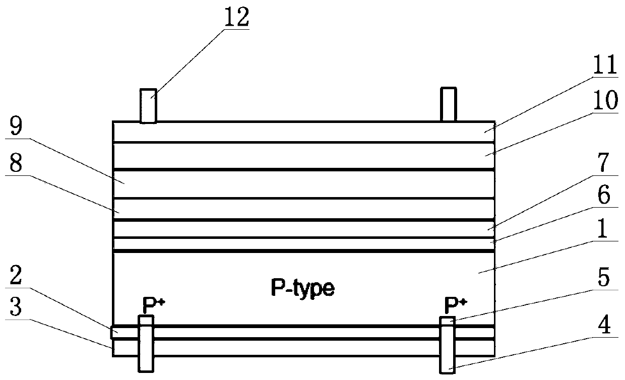
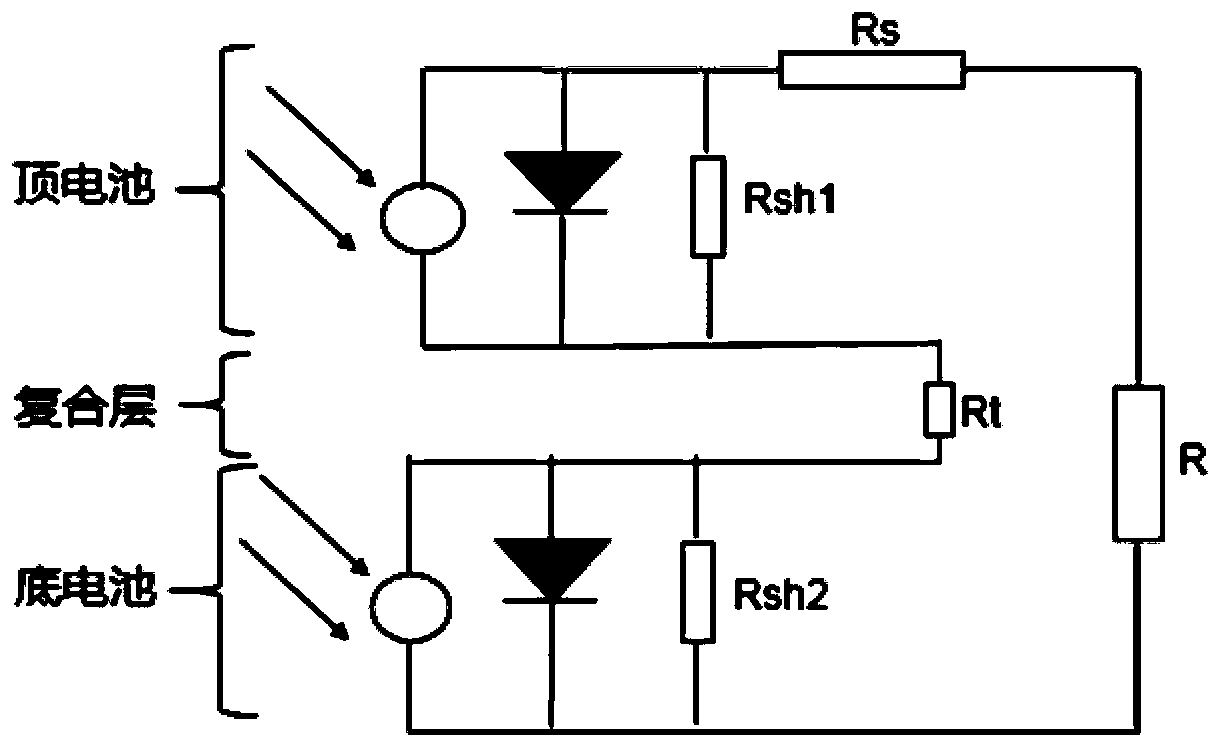
[0039] Such as figure 1 , figure 2 As shown, the silicon-based perovskite double-diode double-sided solar cell of the present embodiment includes a bottom cell, a composite layer 7 and a top cell, and the bottom cell includes a P-type silicon substrate 1, an AlOx thin film layer 2, a SiONx thin film layer 3 and a bottom cell. Electrode 4, AlOx thin film layer 2, and SiONx thin film layer 3 are sequentially prepared on the lower side of P-type silicon substrate 1, and lower electrode 4 passes through AlOx thin film layer 2 and SiONx thin film layer 3 and is connected to P+ re-doped region 5 of P-type silicon substrate 1 , N+ doped layer 6 is prepared on the front side of P-type silicon substrate 1 to form a bottom electric PN junction, and the composite layer is prepared on N+ doped layer 6, and composite layer 7 includes indium tin oxide (ITO), fluor...

Embodiment 2

[0056] The preparation method of the silicon-based perovskite double-diode double-sided solar cell of the present embodiment comprises the following steps:

[0057] 1) Surface cleaning and texture: Use a low-concentration alkaline solution to perform anisotropic corrosion on the P-type silicon substrate 1, and corrode the surface of the P-type silicon substrate 1 to form a pyramid-shaped surface morphology. Reactive alkaline solution: 1.0-1.5wt %NaOH, reaction time: 200-400s, temperature: 70-90℃, reflectivity: 11-12%;

[0058] 2) Diffusion of phosphorus at high temperature: through N 2 Diffusion source POCl 3 The steam is brought into the high-temperature diffusion furnace, and a sufficient amount of O is introduced at the same time 2 After a series of chemical reactions, phosphorus atoms diffuse into the P-type silicon chip to form an N+ doped layer 6, and the N+ doped layer 6 cooperates with the P-type silicon substrate 1 to form a bottom cell PN junction, N 2 Flow: 500-8...

Embodiment 3

[0072] The preparation method of the silicon-based perovskite double-diode double-sided solar cell of the present embodiment comprises the following steps:

[0073] 1) Surface cleaning and texture: Use a low-concentration alkaline solution to perform anisotropic corrosion on the P-type silicon substrate 1, and corrode the surface of the P-type silicon substrate 1 to form a pyramid-shaped surface morphology. Reactive alkaline solution: 1.0-1.5wt %NaOH, reaction time: 200-400s, temperature: 70-90℃, reflectivity: 11-12%;

[0074] 2) Diffusion of phosphorus at high temperature: through N 2 Diffusion source POCl 3 The steam is brought into the high-temperature diffusion furnace, and a sufficient amount of O is introduced at the same time 2 After a series of chemical reactions, phosphorus atoms diffuse into the P-type silicon chip to form an N+ doped layer 6, and the N+ doped layer 6 cooperates with the P-type silicon substrate 1 to form a bottom cell PN junction, N 2 Flow: 500-8...


PUM

PropertyMeasurementUnit
thicknessaaaaaaaaaa
thicknessaaaaaaaaaa
thicknessaaaaaaaaaa

Abstract

The invention relates to a silicon-based perovskite double-diode double-sided solar cell and a preparation method thereof. The battery comprises a bottom battery, a composite layer and a top battery,the bottom cell comprises a P-type silicon substrate, an AlOx film layer, a SiONx film layer and a lower electrode. The AlOx thin film layer and the SiONx thin film layer are sequentially prepared onthe lower side of the P-type silicon substrate. The lower electrode penetrates through the AlOx thin film layer and the SiONx thin film layer and is connected with the P + heavily doped region of theP-type silicon substrate; an N + doping layer is prepared on the front surface of the P-type silicon substrate to form a bottom electric PN junction; the composite layer is prepared on the N + doped layer; the top cell is prepared on the composite layer; the top cell comprises a hole transport layer, a perovskite layer, an electron transport layer and a transparent conductive film layer which aresequentially arranged from bottom to top, wherein the transparent conductive film layer is connected with the upper electrode, the bottom cell and the top cell are connected in series through the composite layer, and the silicon-based perovskite double-diode double-sided solar cell is high in photoelectric conversion efficiency, mature in process and high in industrialization degree.

Description

technical field [0001] The invention relates to a solar cell, in particular to a silicon-based perovskite double-diode double-sided solar cell and a preparation method thereof. Background technique [0002] At present, silicon-based solar cells are the mainstream products in the photovoltaic industry. With the continuous development and innovation of solar cell technology, the conversion efficiency of silicon-based single-diode solar cells has approached the theoretical limit of Shockley-Queisser photovoltaic conversion efficiency; in order to meet the continuous cost reduction and efficiency improvement of the photovoltaic industry The development trend and the early realization of the goal of grid parity require the development and design of new structural solar cells. Among them, the solar cell with double diode structure can not be limited by the theoretical limit of Shockley-Queisser conversion efficiency. The double-diode structure solar cell is composed of two single...

Claims


Application Information

Patent Timeline
Patent Type & Authority Applications(China)
IPC IPC(8): H01L27/30H01L51/42
CPCH10K39/10H10K30/152H10K30/151Y02E10/549
Inventor 康海涛胡燕吴中亚郭万武
Owner JETION SOLAR HLDG
Learn More