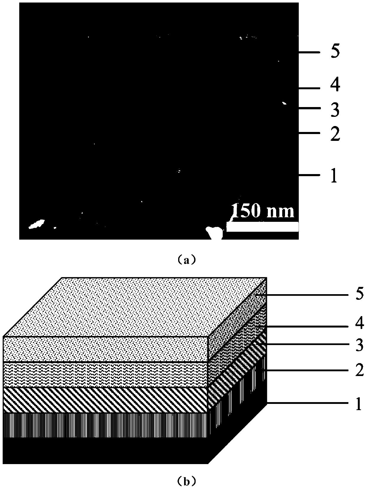
CsPbX<3> perovskite nanocrystalline electroluminescent diode with self-assembled multi-dimensional quantum well
A quantum well and nanocrystalline technology, applied in circuits, electrical components, electric solid devices, etc., can solve the problem of low external quantum efficiency of pure blue light and pure red LED, poor electrical, optical and thermal stability of nanocrystals, and can not achieve practical Application standards and other issues, to achieve the effect of high luminous efficiency and external quantum efficiency of electroluminescent diode LED, good stability and less defects
- Summary
- Abstract
- Description
- Claims
- Application Information
AI Technical Summary
Problems solved by technology
Method used
Image

Examples
Embodiment 1
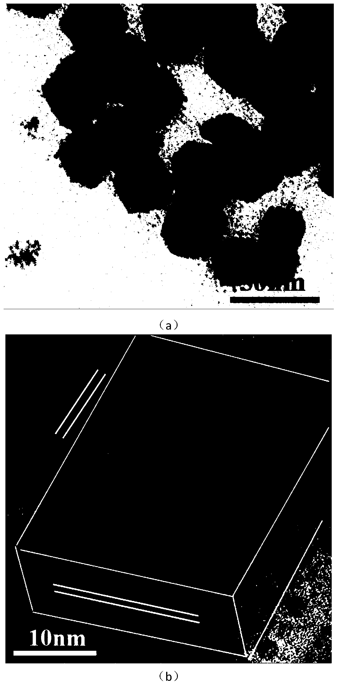
[0031] lead halide (PbX 2 ), oleic acid (OA), and octylamine (OTA) were mixed according to the molar ratio of 1:0.3:0.6, placed in the container of the heating device, stirred, vacuumed, and heated to 100°C to obtain 0.5 mole Concentration of lead precursor solution; cesium carbonate (Cs 2 CO 3 ), oleic acid (OA) was added to octadecene (ODE) according to the molar ratio of 1:0.4, and then placed in a heating device container, stirred, vacuumed, and heated to 100°C to obtain 0.5 molar concentration of Cesium precursor solution; under inert gas protection conditions, the cesium precursor solution is heated to 100°C, and a 0.5 molar concentration of lead precursor solution is injected. Incubate for 60 seconds. During this process, the two-dimensional CsPbX 3 The nanosheets are gradually assembled into nanocrystals with a multidimensional quantum well structure, and the size of the nanocrystals is 20 nanometers. Use an ice bath to quickly cool down the reaction solution to 0°...
Embodiment 2
[0035] lead halide (PbX 2 ), oleic acid (OA), and octylamine (OTA) were mixed according to the molar ratio of 1:0.4:0.8, placed in the container of the heating device, stirred, vacuumed, and heated to 120°C to obtain 1.0 mole Concentration of lead precursor solution; cesium carbonate (Cs 2 CO 3 ), oleic acid (OA) was added into octadecene (ODE) according to the molar ratio of 1:0.5, and then placed in a heating device container, stirred, vacuumed, and heated to 120°C to obtain 0.7 molar concentration of Cesium precursor solution; under inert gas protection conditions, the cesium precursor solution is heated to 120°C, and a lead precursor solution with a concentration of 1.0 molar is injected. Incubate for 40 seconds. During this process, the two-dimensional CsPbX 3 The nanosheets are gradually assembled into nanocrystals with a multidimensional quantum well structure, and the size of the nanocrystals is 30 nanometers. Use an ice bath to quickly cool down the reaction solut...
Embodiment 3
[0039] lead halide (PbX 2 ), oleic acid (OA), and octylamine (OTA) were mixed according to the molar ratio of 1:0.5:1, placed in the container of the heating device, stirred, vacuumed, and heated to 150 ° C to obtain 1.5 moles Concentration of lead precursor solution; cesium carbonate (Cs 2 CO 3 ), oleic acid (OA) was added to octadecene (ODE) according to the molar ratio of 1:0.6, and then placed in a heating device container, stirred, vacuumed, and heated to 150°C to obtain 1.0 molar concentration of Cesium precursor solution; under inert gas protection conditions, the cesium precursor solution is heated to 150°C, and a lead precursor solution with a concentration of 1.5 moles is injected. Incubate for 30 seconds. During this process, the two-dimensional CsPbX 3 The nanosheets are gradually assembled into nanocrystals with a multidimensional quantum well structure, and the size of the nanocrystals is 40 nanometers. Use an ice bath to quickly cool down the reaction soluti...
PUM
| Property | Measurement | Unit |
|---|---|---|
| size | aaaaa | aaaaa |
Abstract
Description
Claims
Application Information
 - R&D
- Intellectual Property
- Life Sciences
- Materials
- Tech Scout
- Unparalleled Data Quality
- Higher Quality Content
- 60% Fewer Hallucinations
Browse by: Latest US Patents, China's latest patents, Technical Efficacy Thesaurus, Application Domain, Technology Topic, Popular Technical Reports.
© 2025 PatSnap. All rights reserved.Legal|Privacy policy|Modern Slavery Act Transparency Statement|Sitemap|About US| Contact US: help@patsnap.com