BCB thickness on-chip monitoring and control method and device
A control method and substrate technology, which are applied to measurement devices, optical devices, phase-influenced characteristic measurement, etc., can solve the problems of measurement accuracy error, sample destructiveness, slow measurement speed, etc. Destructive and complex, easy-to-process effects
- Summary
- Abstract
- Description
- Claims
- Application Information
AI Technical Summary
Problems solved by technology
Method used
Image

Examples
Embodiment 1
[0051] A method for on-chip monitoring and control of BCB thickness in an InP-HBT process, the steps comprising:
[0052] (1) Clean and dry the substrate, spin-coat photoresist on the surface, the adhesive layer has high resolution and is easy to peel off; the photoresist layer is selected from AZ1500 or AZ5214, and the thickness of the adhesive layer is 1um-8um;
[0053] (2) Expose and develop on the subbing layer with deep ultraviolet lithography, and transfer the monitoring pattern on the layout to the subbing layer; the designed monitoring pattern is circular or square, with a diameter or side length of 10um-100um.
[0054] (3) Prepare the metal thin film of monitoring pattern with evaporation stripping process, prepare the epitaxial film of monitoring pattern with dry etching process, prepare the dielectric film of monitoring pattern with vapor deposition process;
[0055] The metal film layer is selected from Ti or Au with a thickness of 10nm-800nm, the epitaxial film la...
Embodiment 2
[0062] like Figure 1-8 As shown, a method for on-chip monitoring and control of BCB thickness in an InP-HBT process, the steps include:
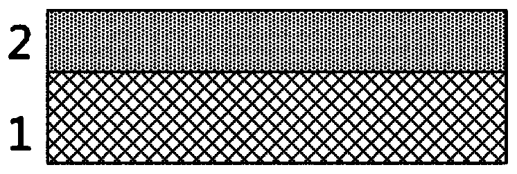
[0063] 1) Select the InP HBT epitaxial substrate 1, wash it with acetone, isopropanol and deionized water, dry it with high-purity nitrogen in a clean room, and spin-coat a 4um thick photoresist 2 on the surface of the substrate, such as figure 1 as shown,
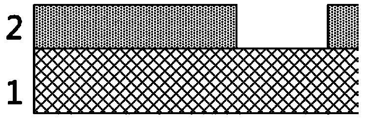
[0064] 2) Use deep ultraviolet lithography technology to expose and develop, and transfer the monitoring pattern on the photoresist plate to the photoresist layer, such as figure 2 shown;
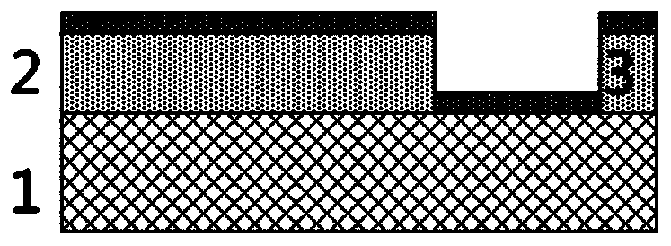
[0065] 3) Utilize the electron beam evaporation process to evaporate a metal Ti layer 3 with a thickness of about 10 nm on the surface of the photoresist, such as image 3 shown;
[0066] 4) Utilize acetone to soak the substrate, peel off the metal layer, and transfer the monitoring pattern to the metal Ti layer 3, such as Figure 4 shown;
[0067] 5) Spin 2um thick BCB glue onto the surface o...
Embodiment 3
[0072] This embodiment step is compared with embodiment 2, and its difference is that the film material of selection is Si 3 N 4 Medium, the specific method is:
[0073] 1) Select an InP HBT epitaxial substrate, wash it with acetone, isopropanol and deionized water, dry it with high-purity nitrogen in a clean room, and grow 100nm Si on the surface of the substrate 3 N 4 medium;
[0074] 2) Spin-coat the photoresist layer, and transfer the monitoring pattern to the photoresist layer by exposure and development;
[0075] 3) Using a dry etching process, the monitoring pattern is transferred from the photoresist layer to the Si 3 N 4 medium layer;
[0076] 4) Spin-coat 2um thick BCB glue on the surface of the substrate, heat it to 250°C in a nitrogen-filled oven for 2 hours, then cool it to room temperature and take it out;
[0077] 5) Find the monitoring pattern on the wafer under the field of view of the objective lens of the film thickness meter, align the center of the ...
PUM
| Property | Measurement | Unit |
|---|---|---|
| Thickness | aaaaa | aaaaa |
| Thickness | aaaaa | aaaaa |
| Thickness | aaaaa | aaaaa |
Abstract
Description
Claims
Application Information
 - R&D
- Intellectual Property
- Life Sciences
- Materials
- Tech Scout
- Unparalleled Data Quality
- Higher Quality Content
- 60% Fewer Hallucinations
Browse by: Latest US Patents, China's latest patents, Technical Efficacy Thesaurus, Application Domain, Technology Topic, Popular Technical Reports.
© 2025 PatSnap. All rights reserved.Legal|Privacy policy|Modern Slavery Act Transparency Statement|Sitemap|About US| Contact US: help@patsnap.com