Organic electroluminescent device

An electroluminescent device and organic light-emitting layer technology, applied in circuits, electrical components, electrical solid-state devices, etc., can solve the problems of reduced yield, increased cost, and complicated process.

Pending Publication Date: 2020-04-28
BEIJING SUMMER SPROUT TECH CO LTD
View PDF7 Cites 20 Cited by
  • Summary
  • Abstract
  • Description
  • Claims
  • Application Information

AI Technical Summary

Problems solved by technology

The disadvantage of this structure is the same as CN 207781602U
Moreover, the near-infrared emission layer in US 20190348628 A1 only accounts for a part of the entire pixel, which requires the use of an additional mask to pattern

Method used


Image

  • Organic electroluminescent device
  • Organic electroluminescent device
  • Organic electroluminescent device

Examples


Embodiment 1

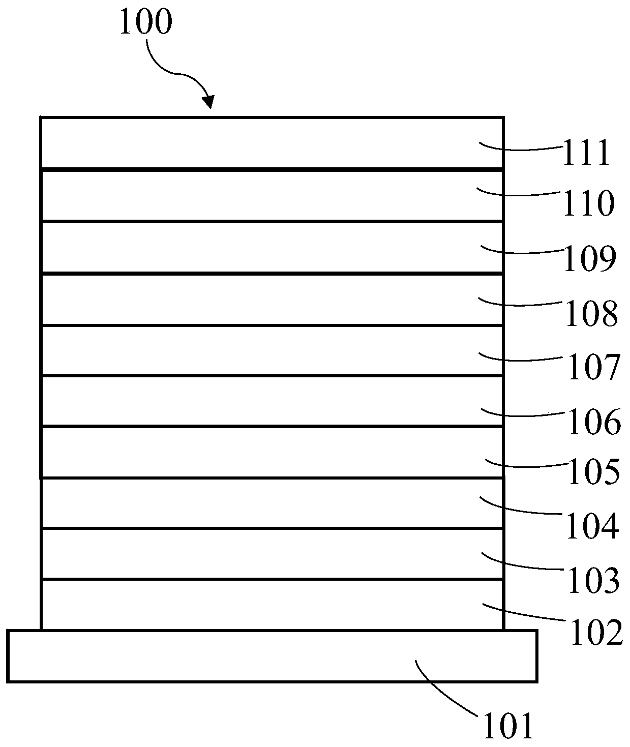
[0070] First, we prepared OLED units that can emit near-infrared and red light. The device structure is as follows: Figure 1a Device 100 is shown. First, the glass substrate 101, on which a patterned 120 nm-thick indium tin oxide (ITO) anode 102 was previously coated, was cleaned with ultrapure water, and the ITO surface was treated with UV ozone and oxygen plasma. Afterwards, the substrate was dried in a nitrogen-filled glove box to remove moisture, then mounted on a stand and loaded into an evaporation chamber. The organic layer specified below, at a vacuum of about 1*10 -6 In the case of Torr, a film is sequentially coated on the ITO anode 102 by thermal evaporation at a rate of 0.01-5 angstroms / second. Firstly, the compound HI was vapor-deposited as a hole injection layer (HIL) 103 with a thickness of 100 angstroms. Compound HT was used as hole transport layer (HTL) 104 with a thickness of 400 angstroms. Compound H-1 was used as an electron blocking layer (EBL) 105 wit...


PUM

PropertyMeasurementUnit
Thicknessaaaaaaaaaa
Thicknessaaaaaaaaaa
Thicknessaaaaaaaaaa

Abstract

The invention discloses an organic electroluminescent device including a substrate, an organic electroluminescent apparatus, and an external electric driving unit. The organic electroluminescent device comprises at least two organic light-emitting layers. Each of the organic light-emitting layers at least comprises a first organic light-emitting layer and a second organic light-emitting layer which emit a first intrinsic peak wavelength and a second intrinsic peak wavelength respectively; the external electric driving unit is connected with a first electrode and a second electrode; when an external electric driving unit provides a first or second working current density for the apparatus, the apparatus can emit a first or second spectrum and generate a first or second light-emitting region, and the regions are overlapped; wherein the first and second spectrum comprise first and second intrinsic peak wavelengths, and ratios of the first and second intrinsic peak wavelengths are different under different working currents; the first intrinsic peak wavelength is less than or equal to 680nm, and the second intrinsic peak wavelength is greater than 680nm and less than or equal to 2000nm.The device integrates multiple light-emitting layers of near-infrared light and visible light and can emit light of different colors under different current densities.

Description

technical field [0001] The invention relates to an organic electroluminescence device. More specifically, it relates to an organic electroluminescent device with both visible light and near-infrared light. Background technique [0002] An organic electroluminescent device (OLED) is composed of a cathode, an anode, and an organic light-emitting material between the cathode and the anode. By applying a voltage across the cathode and anode of the device, the electrical energy is converted into light. It has a wide angle, high contrast and Advantages such as faster response time. Tang and Van Slyke of Eastman Kodak Company reported an organic light-emitting device in 1987, arylamine hole transport layer and three-8-hydroxyquinoline-aluminum layer as electron transport layer and light-emitting layer (Applied Physics Letters, 1987, 51(12):913-915). Green light was emitted from the device after a voltage was applied across it, an invention that set the stage for the development ...

Claims


Application Information

Patent Timeline
IPC IPC(8): H01L51/50H01L27/32G09G3/3233
CPCG09G3/3233H10K59/30H10K50/13
Inventor 谢梦兰高亮庞惠卿
Owner BEIJING SUMMER SPROUT TECH CO LTD
Why Eureka
Try Eureka