
Method for preventing metal ion migration on surface of PCB

A metal ion, PCB board technology

Pending Publication Date: 2020-05-08
苏州晶台光电有限公司
View PDF7 Cites 1 Cited by
  • Summary
  • Abstract
  • Description
  • Claims
  • Application Information

AI Technical Summary

Problems solved by technology

[0004] The existing PCB substrate surface treatment and encapsulation process can better protect the chips and metal lines when the line spacing is wide. However, as the metal lines become thinner and the spacing becomes smaller, the existing These PCB board surface treatment methods have been difficult to effectively protect the active metal (such as Cu) in the lower layer. In some high-humidity and high-temperature environments, metal lines and pads are prone to metal migration.
In addition, the environmental protection requirements are becoming more and more stringent, and the surface treatment methods of PCB boards such as electroplating and chemical plating are becoming more and more restricted.

Method used


Image

  • Method for preventing metal ion migration on surface of PCB
  • Method for preventing metal ion migration on surface of PCB

Examples


Embodiment 1

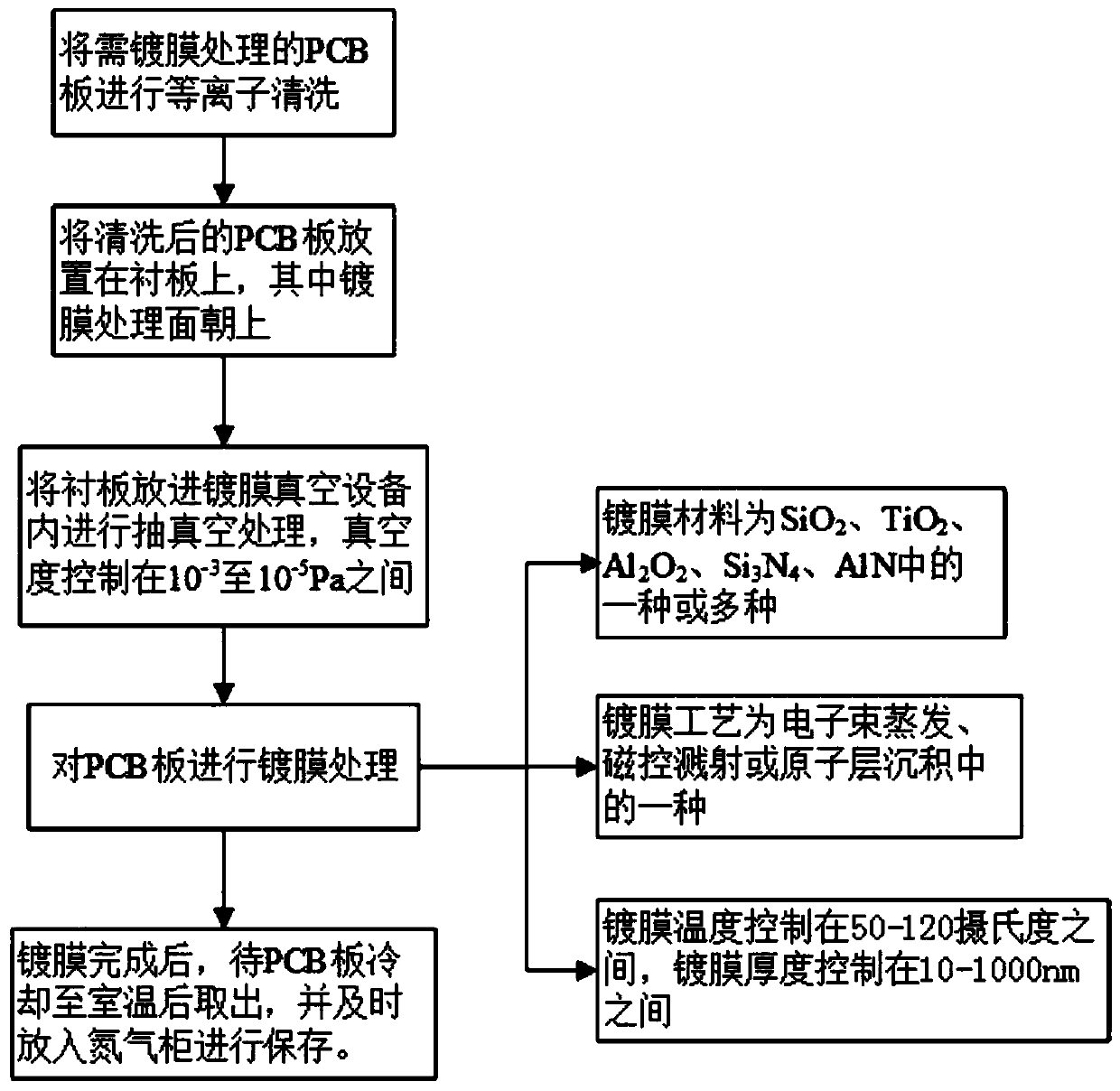
[0027] Such as figure 1 As shown, what the present invention mainly relates to is the vacuum coating process, and the vacuum coating process is used to ensure that the required inert protective layer is prepared uniformly under a low temperature and dust-free environment.

[0028] The preparation method is as follows:

[0029] S1: Plasma cleaning the PCB board to be coated;

[0030] S2: Place the cleaned PCB on the liner, with the coated surface facing up;

[0031] S3: Put the lining board into the coating vacuum equipment for vacuum treatment, and the vacuum degree is controlled at 10 -3 to 10 -5 Between Pa;

[0032] S4: Coating the PCB board, the coating material is SiO 2 、TiO 2 、Al 2 o 2 、Si 3 N 4 , one or more of AlN, the coating process is one of electron beam evaporation, magnetron sputtering or atomic layer deposition, and the coating temperature is controlled between 50-120 degrees Celsius;

[0033] S5: After the coating is completed, take out the PCB board ...


PUM

PropertyMeasurementUnit
Thicknessaaaaaaaaaa

Abstract

The invention relates to the technical field of PCB substrate packaging, in particular to a method for preventing metal ion migration on the surface of a PCB. The method comprises the following steps:carrying out plasma cleaning on a PCB to be subjected to coating treatment, and then placing the PCB on a lining plate, wherein the coating treatment face is upward; placing the lining plate in coating vacuum equipment to be subjected to vacuumizing treatment, and then performing the coating treatment of the PCB; after coating, taking out the PCB after the PCB is cooled to the room temperature, and placing the PCB in a nitrogen cabinet in time to be stored. According to the invention, special surface coating treatment is carried out on the PCB before a chip is installed, and the formed protective layer structure can effectively block the ion migration phenomenon of a metal circuit between metal circuits or bonding pads on the PCB under the multiple influences of moisture, chemical erosion, voltage and the like.

Description

technical field [0001] The invention relates to the technical field of PCB substrate packaging, in particular to a method for preventing the migration of metal ions on the surface of a PCB. Background technique [0002] In recent years, the packaging of IC, MEMS and LED chips has continued to develop in a smaller size direction, which makes the metal lines of the PCB substrate used for packaging more dense, the layout is more complicated, and the corresponding spacing is narrower. These new trends in packaging PCB boards have greatly increased the risk of metal ion migration in packaged electronic products, resulting in failure of the overall packaged electronic product. [0003] The existing methods to prevent metal migration of metal lines and pads on PCB substrates are mainly to perform various chemical or electroplating treatments on PCB metal lines and pads, such as nickel immersion gold, electroplated nickel gold, electroless nickel palladium gold, etc. Then fill the ...

Claims


Application Information

Patent Timeline
IPC IPC(8): H05K3/28
CPCH05K3/28
Inventor 龚文罗志军陈海力黄见
Owner 苏州晶台光电有限公司
Learn More