Inductive coupling device and semiconductor processing device

A technology of inductive coupling and processing equipment, which is applied in the field of inductive coupling devices and semiconductor processing equipment, can solve problems such as limiting effective power absorption, cracking, and thermal effects of dielectric windows, so as to improve the efficiency of inductive coupling power utilization, increase plasma density, Reduce the effect of skin effect

Active Publication Date: 2020-05-22
BEIJING NAURA MICROELECTRONICS EQUIP CO LTD
View PDF6 Cites 1 Cited by
  • Summary
  • Abstract
  • Description
  • Claims
  • Application Information

AI Technical Summary

Problems solved by technology

For inductively coupled plasmas, the increase in power density will lead to two problems: one is that the direction of the induced current generated by the skin effect is opposite to the direction of the coil current, which limits the absorption of effective power; the other is that the high power density leads to the generation of dielectric windows Thermal effect, cracking phenomenon, for planar inductively coupled plasma

Method used


Image

  • Inductive coupling device and semiconductor processing device
  • Inductive coupling device and semiconductor processing device
  • Inductive coupling device and semiconductor processing device

Examples


Example Embodiment

[0036] The specific embodiments of the present invention will be described in detail below with reference to the accompanying drawings. It should be understood that the specific embodiments described herein are only used to illustrate and explain the present invention, and not to limit the present invention.

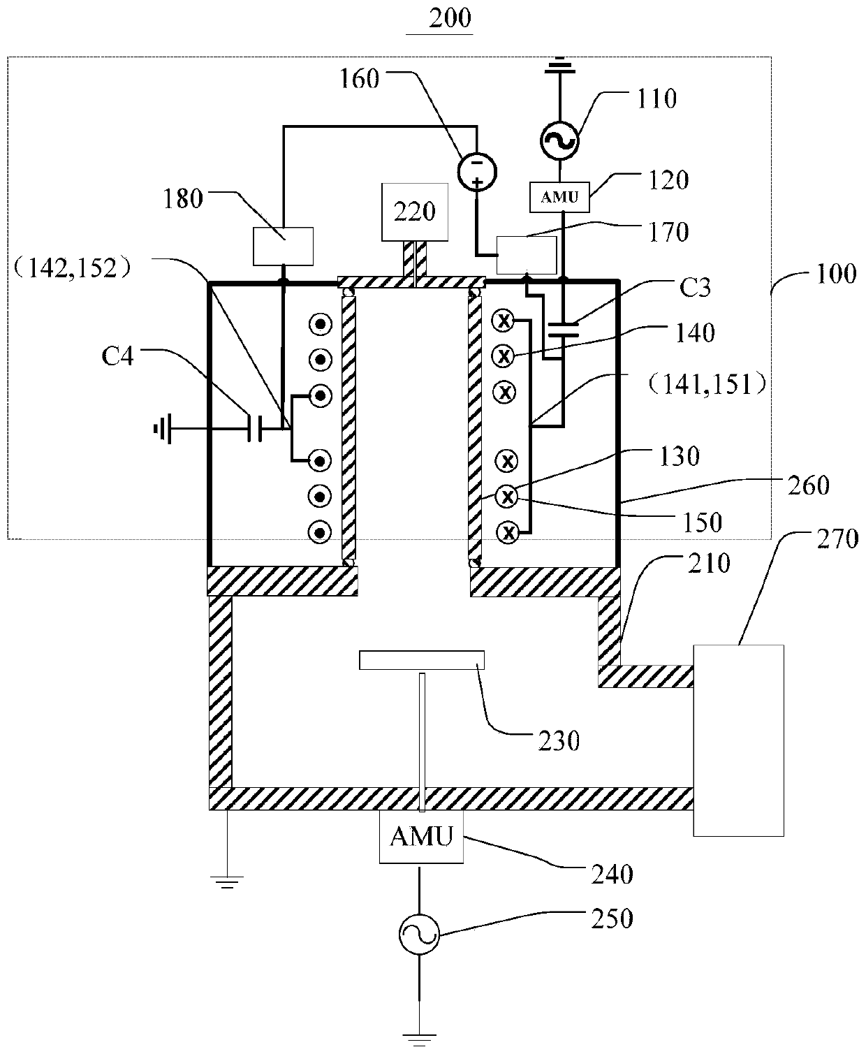
[0037] Such as figure 1 As shown, the first aspect of the present invention relates to an inductive coupling device 100. The inductive coupling device 100 is used in a semiconductor processing equipment 200. The semiconductor processing equipment 200 generally includes a process chamber 210 and a device placed above the process chamber 210. The inductive coupling device 100 proposed in the present invention, the gas inlet system 220 that provides the process gas to the process chamber 210, and the bias electrode 230 located in the process chamber 210, the bias electrode 230 is connected to the process chamber 210 via the bias matching device 240 The bias RF source 250 is el...


PUM


Abstract

The invention discloses an inductive coupling device and a semiconductor processing device. The inductive coupling device comprises a radio frequency power supply, a dielectric cylinder, and at leasttwo groups of radio frequency coils and direct-current power supplies which surround the circumferential side wall of the dielectric cylinder and are sequentially arranged in parallel in the axial direction of the dielectric cylinder, wherein the input end of each group of radio frequency coils is electrically connected with the radio frequency power supply and the first pole of the direct-currentpower supply, and the output end of each group of radio frequency coils is electrically connected with the second pole of the direct-current power supply and is grounded, so that an ionization regioncorresponding to each group of radio frequency coils is formed in the dielectric cylinder. The structure of the plurality of groups of radio frequency coils is designed; under the condition of the same radio frequency power, the current passing through each group of radio frequency coils is reduced, so that the skin effect problem caused by high power density is effectively reduced, the process gas can pass through the two ionization regions in sequence to realize multiple times of ionization, the inductive coupling power utilization efficiency can be effectively improved, and finally, the plasma density can be improved.

Description

technical field [0001] The invention relates to the technical field of semiconductor manufacturing, in particular to an inductive coupling device and a semiconductor processing device including the inductive coupling device. Background technique [0002] With the development of three-dimensional stacked packaging, micro-electro-mechanical system (Micro-Electro-Mechanical System, MEMS) packaging, vertically integrated sensor arrays, and flip-chip bonding technology for mesa metal oxide semiconductor (Metal Oxide Semiconductor, MOS) power devices, Silicon Communications Through Silicon Via (TSV) interconnection technology is receiving more and more attention and research. In order to achieve a higher etching selectivity ratio and etching rate, remote high density plasma (Remote High Density Plasma, Remote HDP) is often used. At this time, the substrate is located downstream of the plasma, with high free radical concentration and low ion density. The loss of the mask layer cau...

Claims


Application Information

Patent Timeline
IPC IPC(8): H01J37/32
CPCH01J37/321H01J37/32357H01J37/3211
Inventor 李兴存
Owner BEIJING NAURA MICROELECTRONICS EQUIP CO LTD
Why Eureka
Try Eureka