A kind of perovskite heterojunction structure and its preparation method and application
Active Publication Date: 2021-09-14
CENT SOUTH UNIV
View PDF9 Cites 0 Cited by
Summary
Abstract
Description
Claims
Application Information
AI Technical Summary
This helps you quickly interpret patents by identifying the three key elements:
Problems solved by technology
Method used
Benefits of technology
Problems solved by technology
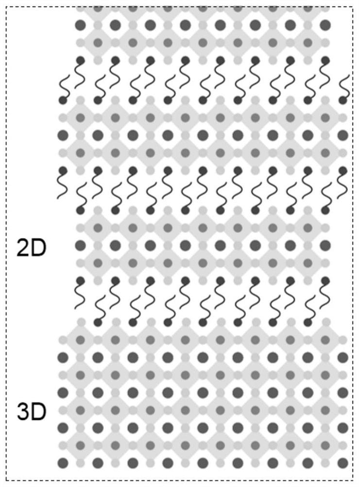
[0004] The interfacial connection between the layered perovskite and the three-dimensional perovskite is formed by the van der Waals force between the organic cations. The three-dimensional perovskite and the layered perovskite are separated by bulky cations, and the contact is not close enough. , the electron clouds do not overlap significantly, and the carrier transport is suppressed. Therefore, so far, devices based on "3D perovskite / layered perovskite" heterojunctions, compared with pure 3D perovskite devices, still sacrifice some of the charge carrier extraction efficiency
Method used
Image
Click on the blue label to locate the original text in one second.
Reading with bidirectional positioning of images and text.
Examples
Embodiment 1
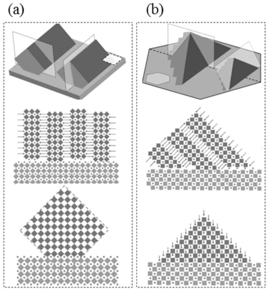
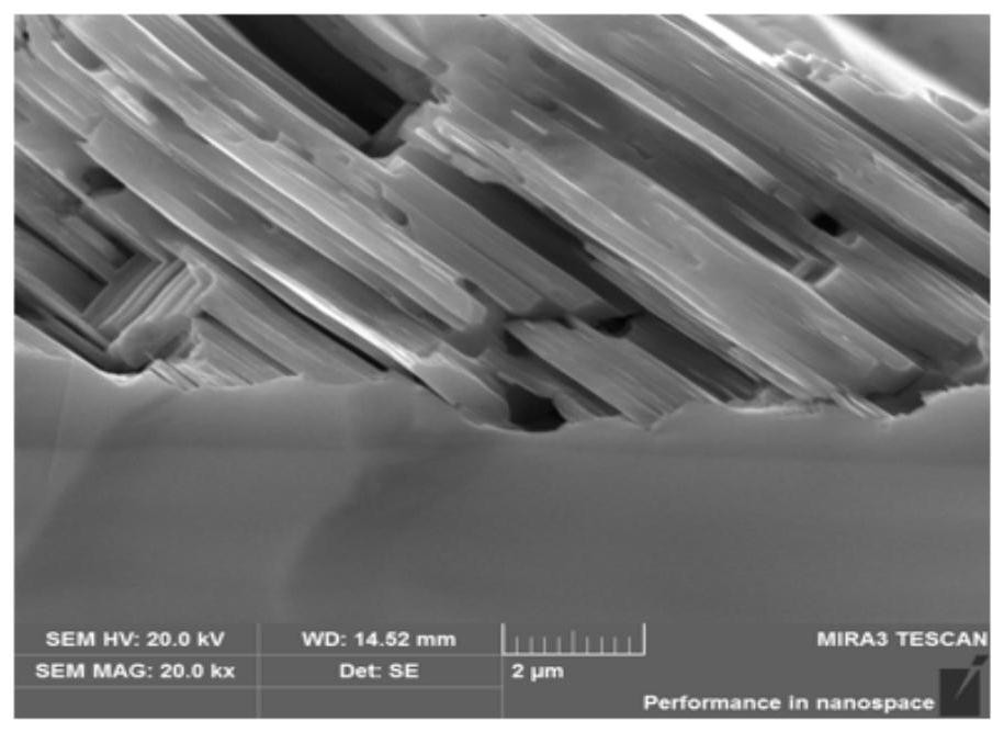
[0037] Example 1 In three-dimensional perovskite MAPbI 3 Epitaxy (BA) 2 MA n-1 Pbn I 3n+1 (n=1,2,3)
[0038] In an embodiment of the present invention, a method for preparing a perovskite heterojunction structure comprises the following steps:
[0040] 1.1) MAI:PbI 2 Mix according to a certain molar ratio, add GBL solvent dropwise to configure a certain concentration of MAPbI 3 Precursor solution, divide the solution into two parts, one part is numbered A, one part is numbered B, then place the solution on the hot stage and stir it with a magnet at room temperature to accelerate the dissolution;
[0041] 1.2) Taking the inversion growth method as an example, put B in a high-temperature oil bath, wait for many crystal seeds to grow in B, then put the crystal seeds in B into A, and then increase the temperature every day, due to the temperature of the solution The increase will lead to a decrease in the solubility o...
Embodiment 2
[0060] Example 2 In three-dimensional perovskite MAPbBr 3 Epitaxy (BA) 2 PbBr 4 (n=1)
[0061] In an embodiment of the present invention, a method for preparing a perovskite heterojunction structure comprises the following steps:
[0063] 1.1) MABr:PbBr 2 Mix according to a certain molar ratio, add DMF solvent dropwise to prepare a solution with a concentration of 550mg / mL, divide the solution into two parts, one part is A, and the other part is B, then place the solution on a hot stage and keep it under room temperature Use magnetic stirring to accelerate dissolution;
[0064] 1.2) Taking the inversion growth method as an example, put B in a high-temperature oil bath, wait for many crystal seeds to grow in B, then put the crystal seeds in B into A, and then increase the temperature of the oil bath every day, because The increase of the solution temperature will lead to a decrease in the solubility of the solution...
Embodiment 3
[0072] Example 3 In three-dimensional perovskite MAPbBr 3 Epitaxy (BA) 2 MAPb 2 I 7 (n=2)
[0073] In an embodiment of the present invention, a method for preparing a perovskite heterojunction structure comprises the following steps:
[0075] 1.1) MABr:PbBr 2 Mix according to a certain molar ratio, add DMF solvent dropwise to prepare a solution with a concentration of 550mg / mL, divide the solution into two parts, one part is A, and the other part is B, then place the solution on a hot stage and keep it under room temperature Use magnetic stirring to accelerate dissolution;
[0076] 1.2) Taking the inversion growth method as an example, put B in a high-temperature oil bath, wait for many crystal seeds to grow in B, then put the crystal seeds in B into A, and then increase the temperature of the oil bath every day, because The increase of the solution temperature will lead to a decrease in the solubility of the sol...
PUM
Abstract
The invention discloses a perovskiteheterojunction structure and its preparation method and application. The heterojunction is composed of three-dimensional perovskite and layered perovskite, and the three-dimensional hybrid perovskite is obtained by lattice matching epitaxy. layered perovskite. The three-dimensional perovskite / layered perovskite heterojunction formed by lattice-matched epitaxial growth in the present invention will induce the layered perovskite to align on the surface of the three-dimensional perovskite, not only making the layered perovskite act as The protective layer of three-dimensional perovskite, at the same time, the two material phases with different electronic structures are combined by chemical bonds, so that the degree of close contact reaches the atomic level, and thus significant electron cloud overlap and crystallization can occur. Lattice modulation, interfacial stress, etc., can form a new interface electronic structure and a new energyband bending phenomenon, which significantly affects the interface charge transfer, energy transfer, carrier migration, recombination and other phenomena.
Description
technical field [0001] The invention belongs to the field of perovskite photoelectric devices, and relates to a perovskite heterojunction structure and its preparation method and application, in particular to a calciumoxide formed at the interface between a three-dimensional perovskite and a layered perovskite due to lattice matching. Titanium heterojunction, and functional devices based on this heterojunction. Background technique [0002] Three-dimensional hybrid perovskites have great potential in the field of photovoltaics due to their high absorption efficiency, long carrier lifetime, high carrier mobility, large carrier diffusion length, and low cost. is one of the most active areas of research. Although the performance of three-dimensional organic-inorganic hybrid solar cells has improved at an astonishing rate from the initial photoelectric conversion efficiency of 3.8% in 2009 to the currently certified 23.7%, and the efficiency has reached commercial silicon sola...
Claims
Application Information
Patent Timeline
Application Date:The date an application was filed.
Publication Date:The date a patent or application was officially published.
First Publication Date:The earliest publication date of a patent with the same application number.
Issue Date:Publication date of the patent grant document.
PCT Entry Date:The Entry date of PCT National Phase.
Estimated Expiry Date:The statutory expiry date of a patent right according to the Patent Law, and it is the longest term of protection that the patent right can achieve without the termination of the patent right due to other reasons(Term extension factor has been taken into account ).
Invalid Date:Actual expiry date is based on effective date or publication date of legal transaction data of invalid patent.

