Mesa etching method for III-nitride semiconductor light-emitting device

A technology for nitride semiconductors and light-emitting devices, which is applied to semiconductor devices, semiconductor lasers, structural details of semiconductor lasers, etc., can solve problems such as difficulty in manufacturing mesa, and achieve the effects of avoiding lattice damage, high crystal quality, and low cost.

Active Publication Date: 2020-06-23
NINGBO INST OF MATERIALS TECH & ENG CHINESE ACADEMY OF SCI
View PDF3 Cites 4 Cited by
  • Summary
  • Abstract
  • Description
  • Claims
  • Application Information

AI Technical Summary

Problems solved by technology

Although traditional wet etching has the advantages of being simple and controllable, less lattice damage, and low cost, but the etching is isotropic, so it is difficult to obtain vertical nitride sidewalls to manufacture mesa

Method used


Image

  • Mesa etching method for III-nitride semiconductor light-emitting device
  • Mesa etching method for III-nitride semiconductor light-emitting device

Examples


Embodiment 1

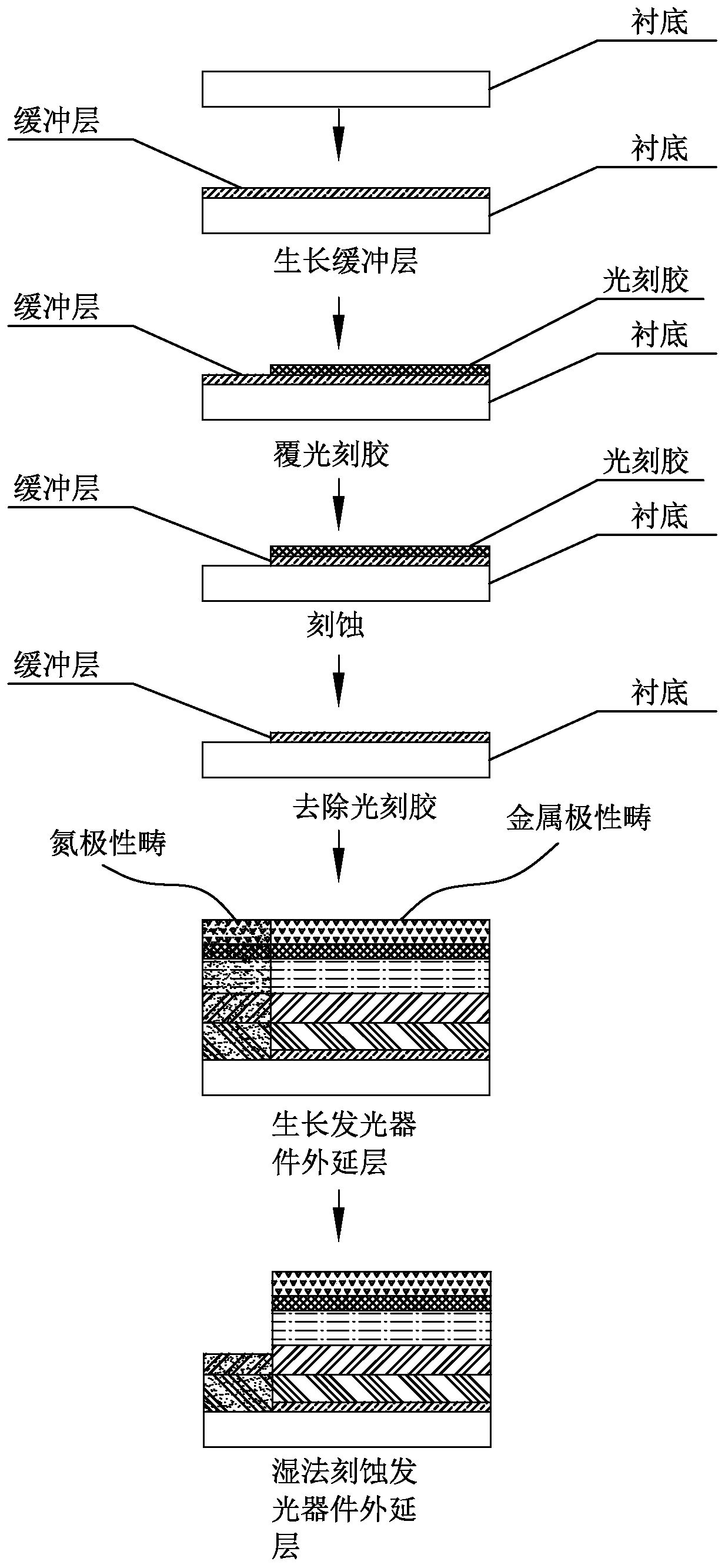
[0026] a) A buffer layer with a thickness of 50 nm is grown on a silicon substrate based on MOCVD technology, and a patterned buffer layer substrate is obtained based on photolithography and plasma etching processes, such as figure 1 As shown, in this embodiment, photolithography is used to remove part of the buffer layer to realize the patterning of the buffer layer, but the patterning scheme is not limited, and any patterning scheme in the existing patterning technology can be used specifically.

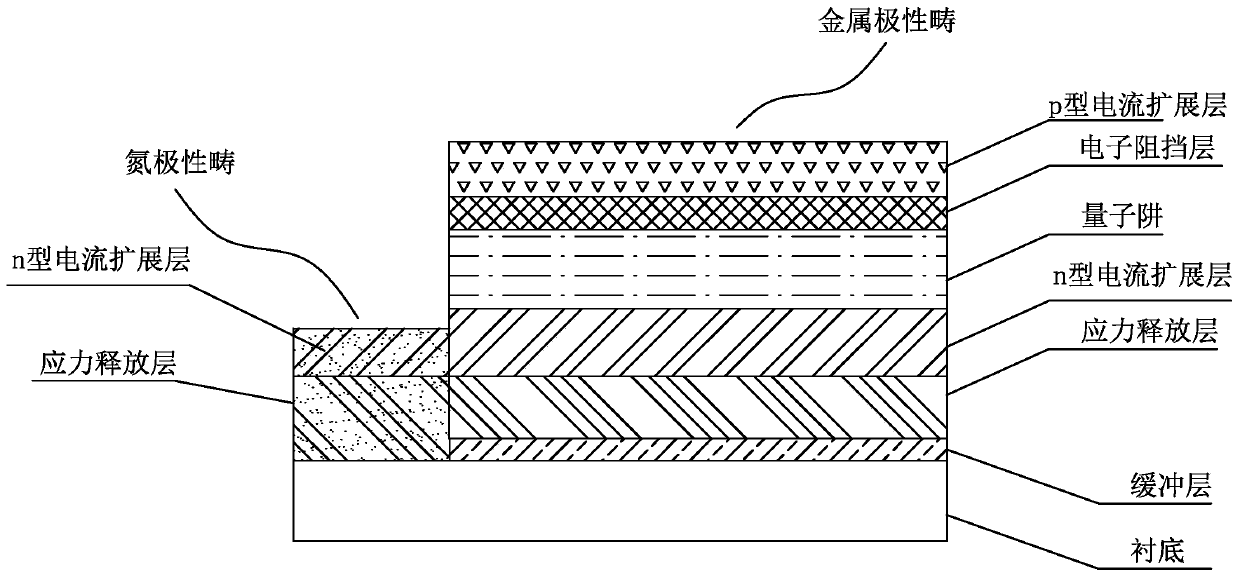
[0027] b) growing an LED epitaxial layer based on a patterned buffer layer substrate. The LED epitaxial layer is sequentially composed of an AlN stress release layer, an n-type current spreading layer, a multilayer quantum well, an electron blocking layer, and a p-type current spreading layer from the bottom layer to the top layer, such as figure 2 shown. The portion of the LED epitaxial layer corresponding to the buffer layer on the substrate is a metal polar domain, and the por...

Embodiment 2

[0032] a) A buffer layer with a thickness of 5 nm was grown on a sapphire substrate based on MBE technology, and a patterned buffer layer substrate was obtained based on photolithography and KOH etching processes.

[0033] b) growing a laser diode epitaxial layer based on a patterned buffer layer substrate. The epitaxial layer of the laser diode is sequentially composed of an AlGaN stress release layer, an n-type current spreading layer, a waveguide layer, a multilayer quantum well, an electron blocking layer, a waveguide layer, and a p-type current spreading layer from the bottom layer to the top layer; the laser diode epitaxial layer The part corresponding to the buffer layer on the substrate is the metal polar domain, and the part corresponding to the no buffer layer on the substrate is the nitrogen polar domain.

[0034] c) Using H at 70°C 3 PO 4 / H 2 o 2 The solution (3M, 0.5M respectively) etched the laser diode epitaxial layer for 5 minutes, the nitrogen polar domai...


PUM


Abstract

The invention discloses a mesa etching method for an III-nitride semiconductor light-emitting device. The method comprises the steps of firstly, epitaxially growing a buffer layer on a substrate, etching the buffer layer to obtain a patterned buffer layer substrate, and epitaxially growing a light-emitting device epitaxial layer with a transverse polarity structure on the patterned buffer layer substrate, wherein the transverse polarity structure comprises a nitrogen polarity domain and a metal polarity domain; and then etching the non-inert polarity domain by adopting a wet etching process according to the inert difference of the nitrogen polarity domain and the metal polarity domain in the etching liquid. According to the invention, a device mesa without plasma damage can be obtained; and the conversion efficiency of the III-nitride light-emitting device is improved, and the manufacturing cost is reduced.

Description

technical field [0001] The invention relates to the technical field of preparation of semiconductor light emitting devices, in particular to a method for etching a mesa of a group III nitride semiconductor light emitting device. Background technique [0002] Group III nitride light-emitting devices such as LEDs and laser diodes, as a new generation of solid-state light sources, have the characteristics of small size, low power consumption and long life. It has broad application prospects and is the best solution to replace traditional incandescent lamps, fluorescent lamps and high-pressure mercury lamp ultraviolet light sources. The preparation of traditional lateral nitride-based light-emitting devices includes steps such as thin film epitaxy, mesa etching, electrode deposition, passivation treatment, packaging and testing. One of the important links is the mesa etching of the light emitting device. Part of the p-type current spreading layer and the active region are remo...

Claims


Application Information

Patent Timeline
IPC IPC(8): H01L33/00H01L33/06H01L33/12H01L33/14H01S5/02
CPCH01L33/007H01L33/06H01L33/12H01L33/145H01S5/0203
Inventor 徐厚强蒋洁安郭炜叶继春
Owner NINGBO INST OF MATERIALS TECH & ENG CHINESE ACADEMY OF SCI
Why Eureka
Try Eureka