Organic electroluminescent device comprising dopant material and plurality of host materials
A technology of electroluminescent devices and host materials, which is applied in the direction of organic semiconductor devices, electric solid devices, semiconductor devices, etc., can solve problems such as unattended coordination, and achieve the effect of improving performance and improving lifespan
- Summary
- Abstract
- Description
- Claims
- Application Information
AI Technical Summary
Problems solved by technology
Method used
Image

Examples
Embodiment 1-1
[0150] Example 1-1: Preparation of an organic electroluminescent device comprising the material combination of the present invention.
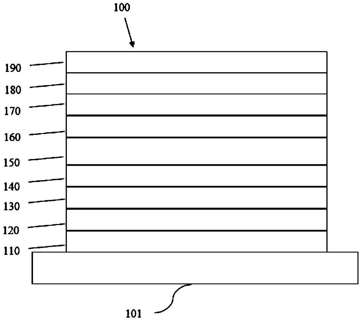
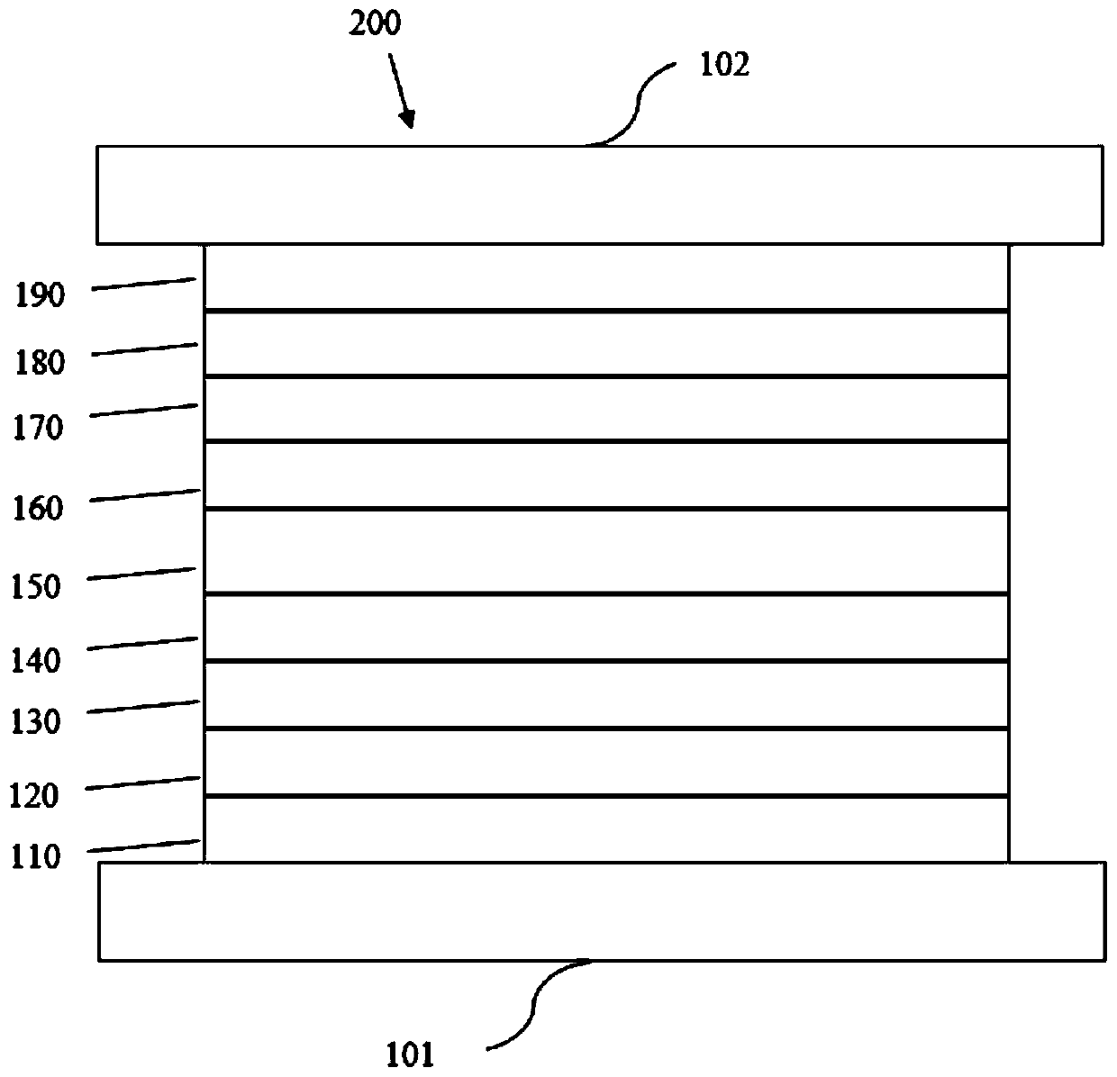
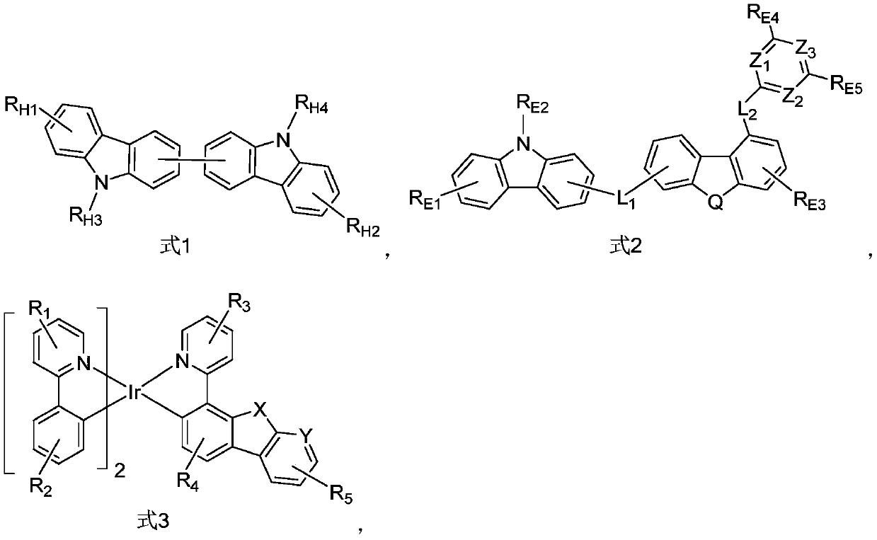
[0151] First, a glass substrate with an 80 nm thick indium tin oxide (ITO) anode was cleaned and then treated with UV ozone and oxygen plasma. After processing, the substrate was dried in a nitrogen-filled glove box to remove moisture, and then mounted on a substrate holder and loaded into a vacuum chamber. The organic layer specified below, at a vacuum of about 10 -8 In the case of Torr, the evaporation is sequentially carried out on the ITO anode by thermal vacuum at a rate of 0.2-2 angstroms / second. Compound HI was used as a hole injection layer (HIL) with a thickness of 100 angstroms. Compound HT was used as a hole transport layer (HTL) with a thickness of 350 angstroms. Compound H-25 was used as an electron blocking layer (EBL) with a thickness of 50 Angstroms. Then compound D-174 is doped in the first host compound H-25 and the secon...
Embodiment 2-1
[0165] Example 2-1: The same preparation method as Example 1-1, except that the dopant compound D-125 used as the dopant compound in the light-emitting layer accounts for 8% of the total weight of the light-emitting layer .
PUM
| Property | Measurement | Unit |
|---|---|---|
| Thickness | aaaaa | aaaaa |
Abstract
Description
Claims
Application Information
 - R&D
- Intellectual Property
- Life Sciences
- Materials
- Tech Scout
- Unparalleled Data Quality
- Higher Quality Content
- 60% Fewer Hallucinations
Browse by: Latest US Patents, China's latest patents, Technical Efficacy Thesaurus, Application Domain, Technology Topic, Popular Technical Reports.
© 2025 PatSnap. All rights reserved.Legal|Privacy policy|Modern Slavery Act Transparency Statement|Sitemap|About US| Contact US: help@patsnap.com