Method for preparing cavity confinement in-situ growth large-area quasi-monocrystalline perovskite thin film

An in-situ growth and perovskite technology, which is applied in semiconductor/solid-state device manufacturing, photovoltaic power generation, electrical components, etc., can solve the problems that are not conducive to the removal of single-crystal perovskite films, are not conducive to high efficiency, and have high resistance , to achieve the effect of being conducive to commercial large-scale production, promoting uniform and rapid growth, and the method is simple and effective

Active Publication Date: 2020-07-24
QUANZHOU NORMAL UNIV
View PDF10 Cites 1 Cited by
  • Summary
  • Abstract
  • Description
  • Claims
  • Application Information

AI Technical Summary

Problems solved by technology

However, the substrate material used in this method does not contain a carrier transport layer, that is, the single crystal perovskite film is not directly grown in situ on the surface of the carrier transport layer; and the method uses the substrate to form a two-dimensional confinement structure, The single-crystal perovskite film is grown between two substrates, and has the same bonding force as the two substrates, which is not conducive to the removal of the single-crystal perovskite film from a certain substrate; in addition, the large-area substrate material does not Contains buried metal electrodes, directly applied to photovoltaic devices, the resistance is very large, which is not conducive to obtaining high-efficiency devices

Method used


Image

  • Method for preparing cavity confinement in-situ growth large-area quasi-monocrystalline perovskite thin film

Examples


Embodiment 1

[0028] (1) FA 0.85 MA 0.15 PB 2.55 Br 0.45Preparation of perovskite precursor solution: mix 1.02mol FAI, 1.02mol PbI 2 , 0.18mol MABr and 0.18mol PbBr 2 Add it into 1L γ-butyrolactone, stir at 80°C for 6 hours, and prepare FA with a total concentration of 1.2mol / L 0.85 MA 0.15 PB 2.55 Br 0.45 Perovskite precursor (among them, MA + for CH 3 NH 3 + ,FA + for HC (NH 2 ) 2 + );

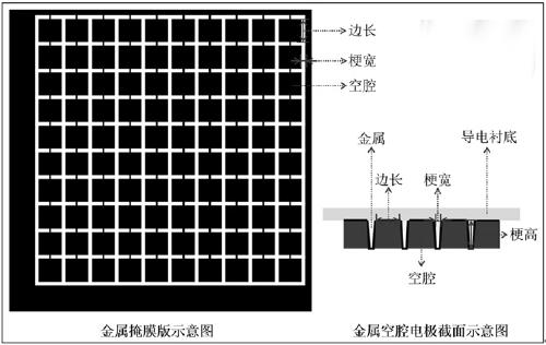
[0029] (2) Construction of the substrate containing aminated graphene quantum dots: on a cleaned transparent conductive substrate of 15 cm × 15 cm, the vacuum thermal evaporation method was used to use a square mask with a side length of 10 mm and a stem width of 0.05 mm. film plate, prepare a square tin metal cavity electrode, its side length, stem width, and stem height are 10 mm, 0.05 mm, and 300 nanometers; Prepare a 100nm-thick tin dioxide electron transport layer on the surface of the cavity electrode; finally, electrophoresis is used to deposit aminated graphene quantum dots on the...

Embodiment 2

[0033] (1) FA 0.85 MA 0.15 PB 2.55 Br 0.45 Preparation of perovskite precursor solution: mix 1.02mol FAI, 1.02mol PbI 2 , 0.18mol MABr and 0.18mol PbBr 2 Add it into 1L γ-butyrolactone, stir at 80°C for 6 hours, and prepare FA with a total concentration of 1.2mol / L 0.85 MA 0.15 PB 2.55 Br 0.45 Perovskite precursor (among them, MA + for CH 3 NH 3 + ,FA + for HC (NH 2 ) 2 + );

[0034] (2) Construction of substrates containing thiolated graphene quantum dots: On a cleaned transparent conductive substrate of 15 cm × 15 cm, vacuum thermal evaporation is used to utilize a regular hexagon with a side length of 10 mm and a stem width of 0.05 mm. A regular hexagonal titanium metal cavity electrode is prepared by using a mask plate, and its side length, stem width, and stem height are 10 mm, 0.05 mm, and 300 nm, respectively; Prepare a 100nm-thick titanium dioxide electron transport layer on the surface of the titanium metal cavity electrode; finally, electrophoresis i...

Embodiment 3

[0038] (1) MAPbI 3 Preparation of perovskite precursor solution: MAI and PbI 2 Add it into a mixed solvent of N,N-dimethylformamide and dimethyl sulfoxide with a volume ratio of 4:1 in an equimolar ratio, stir at 70°C for 6 hours, and prepare MAPbI with a concentration of 1.2mol / L 3 Perovskite precursor (among them, MA + for CH 3 NH 3 + );

[0039] (2) Construction of the substrate containing aminated graphene quantum dots: on a cleaned transparent conductive substrate of 15 cm × 15 cm, the vacuum thermal evaporation method was used to use a square mask with a side length of 10 mm and a stem width of 0.05 mm. stencil (eg figure 1 shown), prepare a square tin metal cavity electrode, whose side length, stem width, and stem height are 10 mm, 0.05 mm, and 200 nm, respectively; Prepare a 100nm-thick tin dioxide electron transport layer on the surface of the cavity electrode; finally, electrophoresis is used to deposit aminated graphene quantum dots on the surface of the tin ...


PUM

PropertyMeasurementUnit
thicknessaaaaaaaaaa
thicknessaaaaaaaaaa
areaaaaaaaaaaa

Abstract

The invention discloses a method for preparing a cavity confinement in-situ growth large-area quasi-monocrystalline perovskite thin film. The method comprises the following steps: firstly, constructing a metal cavity electrode with a specific shape and specification on a large-area transparent conductive substrate so as to reduce an internal resistance of a device; then producing a carrier transport layer on the surface; depositing functionalized graphene quantum dots; and finally performing cavity confinement in-situ growth of a perovskite thin film, and promoting uniform and rapid growth ofquasi-monocrystalline perovskite by using a poor solvent standing method to prepare the large-area quasi-monocrystalline perovskite thin film. The quasi-monocrystalline perovskite thin film obtained by the method has advantages of a large area, few grain boundaries, few defects, a controllable thickness and the low internal resistance, and can be directly applied to photovoltaic devices.

Description

technical field [0001] The invention belongs to the technical field of thin-film solar cells, and in particular relates to a method for preparing a large-area quasi-single-crystal perovskite thin film grown in situ in a cavity confinement. Background technique [0002] In recent years, perovskite solar cells (PSCs) have attracted extensive attention from both academia and industry due to the unique optoelectronic properties and low fabrication cost of organic-inorganic hybrid perovskite materials, bringing new opportunities to the field of photovoltaics. development opportunities. From 2009 to now, PSC's laboratory photoelectric conversion efficiency has been refreshed from 3.8% in 2009 to 25.2% in 2019. However, most of these certified or reported high-efficiency PSCs are based on relatively small areas (generally 0.1cm 2 , some as small as 0.03cm 2 ). Spin-coating technology is a low-cost and easy-to-operate technology that can achieve a total device area of ​​100cm 2...

Claims


Application Information

Patent Timeline
Patent Type & Authority Applications(China)
IPC IPC(8): H01L51/42H01L51/44H01L51/46H01L51/48
CPCH10K71/15H10K71/12H10K85/30H10K30/81H10K30/00Y02E10/549
Inventor 肖尧明
Owner QUANZHOU NORMAL UNIV
Why Eureka
Try Eureka