Preparation method of silicon-based size-controllable beta-Ga2O3 nanowire
A technology of -ga2o3 and nanowires, which is applied in the field of adjusting the diameter of gallium oxide nanowires, can solve the problems of small contact area between film-based detectors and incident light, many internal structural defects, and large leakage current of devices, so it is suitable for popularization and use , Reduce the influence of grain boundaries and defects, and the effect of fast response
- Summary
- Abstract
- Description
- Claims
- Application Information
AI Technical Summary
Problems solved by technology
Method used
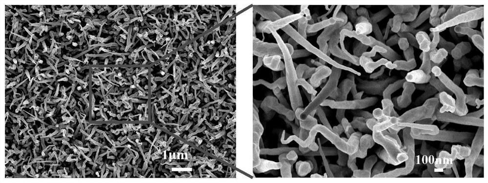
Image

Examples
Embodiment 1
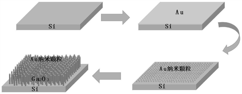
[0032] In this embodiment, a 10nm Au catalytic layer is prepared on a single crystal (100) Si substrate. According to the calculation method of the metal purity according to the impurity concentration ratio contained in the metal, high-purity Au with a purity of 99.999% is selected as the electron beam evaporation method. materials; before sputtering, the Au catalytic layer was annealed at 600°C, and then the temperature was raised to 700°C for formal sputtering of Ga 2 o 3 ; 2 o 3 The purity of the target material is 99.99%, and finally it is annealed in situ at 700°C.
[0033] A Si-based β-Ga 2 o 3 A nanowire size-controllable preparation method, comprising the following steps:
[0034] (1) Substrate cleaning and pretreatment:
[0035] Select a single crystal (100) Si substrate with a size of 20 mm × 20 mm and a thickness of 0.5 mm; the substrate is ultrasonicated in deionized water, acetone, absolute ethanol and deionized water for 5 min, and then diluted in Pickling...
Embodiment 2
[0045] This embodiment is basically the same as Embodiment 1, especially in that:
[0046] In this embodiment, a 20nm-thick Au catalytic layer is prepared on a single crystal (100) Si substrate. According to the calculation method of the metal purity according to the impurity concentration ratio contained in the metal, high-purity Au with a purity of 99.999% is selected as the electron beam Evaporated materials; before sputtering, the Au catalyst layer is subjected to 600°C spheroid annealing treatment, and then the temperature is raised to 700°C for formal sputtering of Ga 2 o 3 ; 2 o 3 The purity of the target material is 99.99%, and finally it is annealed in situ at 700°C.
[0047] A Si-based β-Ga 2 o 3 A nanowire size-controllable preparation method, comprising the following steps:
[0048] (1) Substrate cleaning and pretreatment:
[0049] Select a single crystal (100) Si substrate with a size of 20 mm × 20 mm and a thickness of 0.5 mm; the substrate is ultrasonicat...
Embodiment 3
[0059] This embodiment is basically the same as Embodiment 1, especially in that:
[0060] In this embodiment, a 30nm Au catalytic layer is prepared on a single crystal (100) Si substrate. According to the calculation method of the metal purity according to the impurity concentration ratio contained in the metal, high-purity Au with a purity of 99.999% is selected as the electron beam evaporation method. s material. Before sputtering, the Au catalytic layer was spheroidized and annealed at 600°C, and then the temperature was raised to 700°C for formal sputtering of Ga 2 o 3 . Ga 2 o 3 The purity of the target material is 99.99%, and finally it is annealed in situ at 700°C.
[0061] A Si-based β-Ga 2 o 3 A nanowire size-controllable preparation method, comprising the following steps:
[0062] (1) Substrate cleaning and pretreatment:
[0063] Select a single crystal (100) Si substrate with a size of 20 mm × 20 mm and a thickness of 0.5 mm; the substrate is ultrasonicate...
PUM
| Property | Measurement | Unit |
|---|---|---|
| thickness | aaaaa | aaaaa |
| thickness | aaaaa | aaaaa |
| diameter | aaaaa | aaaaa |
Abstract
Description
Claims
Application Information