
Electromagnetic integrated MEMS scanning micromirror

A scanning micromirror, electromagnetic technology, applied in optical components, optics, instruments, etc., can solve the problems of unfavorable development of spectrometer portability, small contact area at the connection, poor structural stability, etc., to save coil materials, reduce Package volume, the effect of reducing the volume

Inactive Publication Date: 2020-08-04
SOUTHWEST UNIVERSITY
View PDF11 Cites 0 Cited by
  • Summary
  • Abstract
  • Description
  • Claims
  • Application Information

AI Technical Summary

Problems solved by technology

[0003] The patent No. CN105301764B discloses a "MOEMS scanning grating micromirror system" applied to near-infrared spectrometers. The micromirror system has the following disadvantages: (1) Two torsion beams are arranged symmetrically, and the silicon substrate is wound around the torsion beams. Rotation, the central axis of the silicon substrate rotation is parallel to the length direction of the torsion beam, and the two ends of the torsion beam are respectively connected to the silicon substrate and the fixed frame. Small size, poor structural stability, easy to crack or even break due to the influence of processing technology and working environment, which is not conducive to the development of portability of the spectrometer; (2) It uses bilateral drive to realize the rotation of the silicon substrate, requiring two peripherals Permanent magnets lead to a large system volume; (3) The driving coil and angle sensing coil are arranged in multiple turns in the form of involutes, and the coil structure is complicated. The sensing coil occupies too many coils, which brings challenges to the process and causes waste of materials

Method used


Image

  • Electromagnetic integrated MEMS scanning micromirror
  • Electromagnetic integrated MEMS scanning micromirror
  • Electromagnetic integrated MEMS scanning micromirror

Examples


Embodiment 1

[0028] Such as figure 1 and figure 2 As shown, the present embodiment provides an electromagnetic integrated MEMS scanning micromirror, which is integrated and manufactured through MEMS processing technology, including a fixed frame 1 and a drive coil 7 and an angle sensing coil 6 integrated on the inside of the fixed frame 1 and integrated on the back. The monotectic silicon-based micromirror plate 4 is connected between the fixed frame 1 and the partial crystal silicon-based micromirror plate 4 with a connecting plate 3 extending along one side of the partial crystal silicon-based micromirror plate 4 .

[0029] Specifically, the front and back of the monotectic silicon-based micromirror plate 4 are rectangular, and the surface area is 7*6mm 2 , the thickness is 0.4mm. The fixed frame 1 provides freedom constraints and supports for the work of the scanning micromirror. The size of the fixed frame 1 is designed corresponding to the size of the monomorphic silicon-based micr...

Embodiment 2

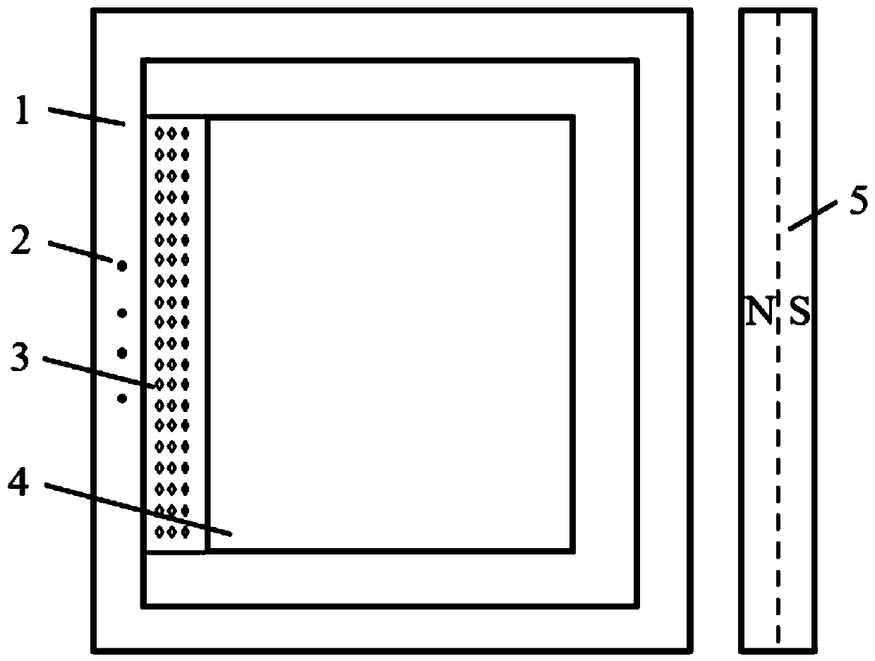
[0036] Such as image 3 As shown, the difference between the second embodiment and the first embodiment lies in the specific structure of the connecting plate 3 . In the second embodiment, the connecting plate 3 is provided with holes arranged in a grid to improve the bending deflection performance of the connecting plate 3 .

Embodiment 3

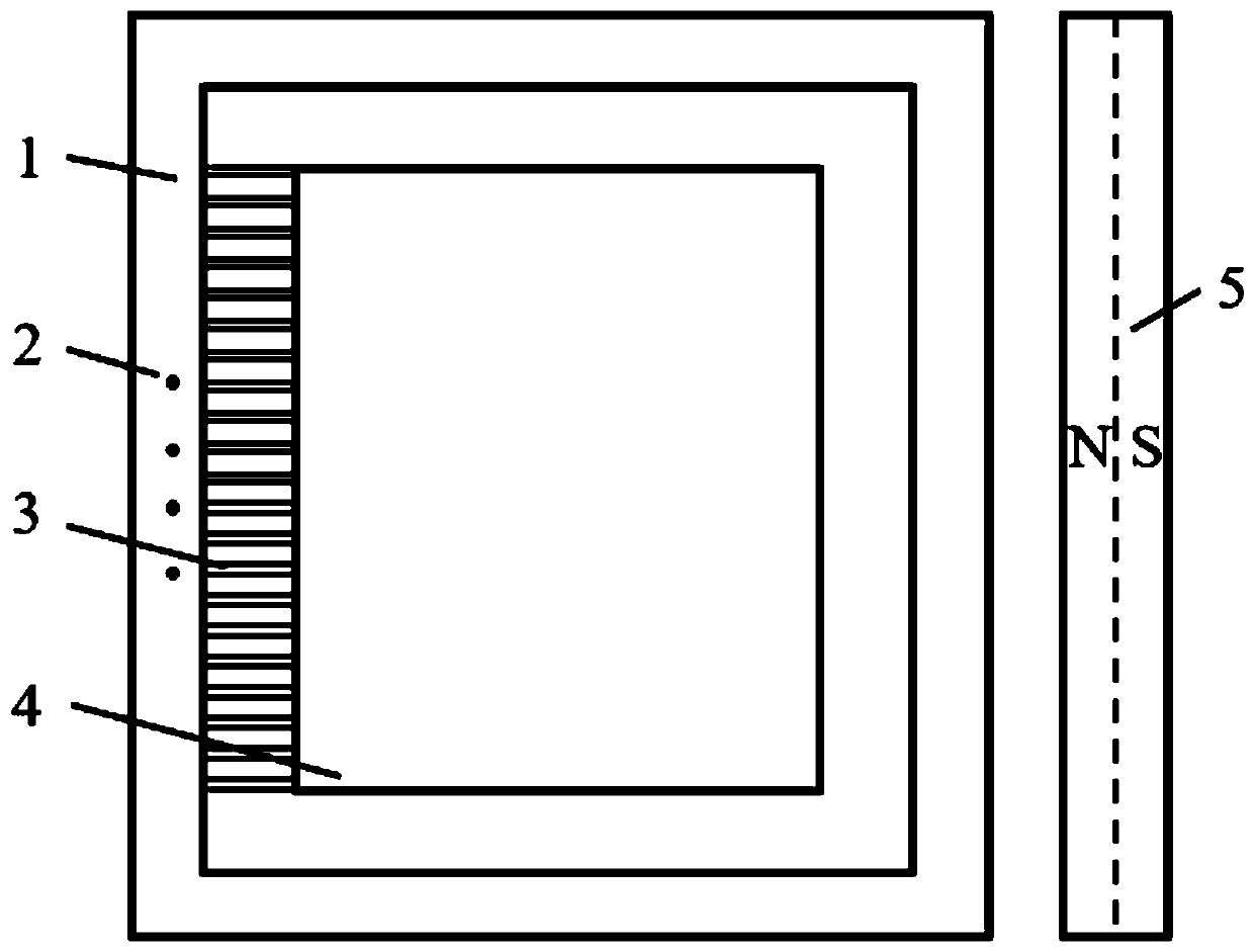
[0038] Such as Figure 4 As shown, the difference between the third embodiment and the first embodiment is that the specific structure of the connecting plate 3 is different. In the third embodiment, the connecting plate 3 is provided with a plurality of parallel equidistant rectangular grooves to improve the bending deflection performance of the connecting plate 3 .

[0039]As an improvement of the above-mentioned embodiment, the drive coil 7 is stacked with multiple layers, and the driving operation of the scanning micromirror is related to the magnitude of the drive current and the strength of the magnetic field. The increase in the number of layers of the drive coil 7 can effectively reduce the resistance of the drive coil 7, and accordingly it will last forever. The volume of the magnet 5 can be reduced, thereby reducing the package volume of the scanning micromirror. In order to enhance the signal output of the angle sensing coil 6 , the angle sensing coil 6 may also be...


PUM

PropertyMeasurementUnit
Surface areaaaaaaaaaaa
Thicknessaaaaaaaaaa

Abstract

The invention relates to an electromagnetic integrated MEMS scanning micromirror, and belongs to the technical field of micro-optical-electro-mechanical systems. The electromagnetic integrated MEMS scanning micromirror comprises a fixed frame and a monotectic silicon-based micro-mirror plate arranged on the inner side of the fixed frame and integrated with a driving coil and an angle sensing coilon the back surface, wherein a connecting plate extending along one side edge of the monotectic silicon-based micro-mirror plate is connected between the fixed frame and the monotectic silicon-based micro-mirror plate. The driving coil and the angle sensing coil are both non-closed rectangular single loops and are distributed in parallel at equal intervals in a striped mode in the extending direction parallel to the connecting plate. The connecting plate is stable in structure and not prone to breakage; only one permanent magnet needs to be arranged externally, and the occupied size is reduced; and through the driving coil and the angle sensing coil which are distributed in parallel in a striped manner, coil materials are saved, and power consumption, processing difficulty and cost are reduced.

Description

technical field [0001] The invention belongs to the technical field of micro-opto-electromechanical systems, and relates to an electromagnetic integrated MEMS scanning micromirror. Background technique [0002] MEMS scanning micromirror refers to an optical single chip that uses optical MEMS (Micro-Electro-Mechanical Systems, Micro-Opto-Electro-Mechanical Systems) manufacturing technology to integrate a micro-optical mirror and a driver, with MEMS scanning micromirror as the core component. The developed spectral analysis technology can qualitatively and quantitatively detect the components and contents of unknown substances, and has been widely used in many fields such as consumer electronics, industrial and agricultural production, national defense and military affairs. The scanning micromirror has carried out in-depth research. [0003] The patent No. CN105301764B discloses a "MOEMS scanning grating micromirror system" applied to near-infrared spectrometers. The micromir...

Claims


Application Information

Patent Timeline
IPC IPC(8): G02B26/08G02B26/10
CPCG02B26/0808G02B26/0875G02B26/10
Inventor 顾雯雯陈亮李丽黄磊
Owner SOUTHWEST UNIVERSITY
Learn More