A silicon carbide based co 2 Reflective film and preparation method thereof

A silicon carbide, reflective film technology, applied in mirrors, instruments, optics, etc., can solve technical difficulties and other problems

Active Publication Date: 2021-11-02
NANJING WAVELENGTH OPTO ELECTRONICS SCI & TECH CO LTD
View PDF7 Cites 0 Cited by
  • Summary
  • Abstract
  • Description
  • Claims
  • Application Information

AI Technical Summary

Problems solved by technology

Due to its unique crystal structure, the surface of silicon carbide presents a honeycomb structure. Although the surface roughness of silicon carbide has reached within 0.02 microns, how to coat the film firmly on this lens and how to reduce the damage caused by the crystal structure on the surface of the lens The problem of scattering is still a technical difficulty

Method used


Image

  • A silicon carbide based co  <sub>2</sub> Reflective film and preparation method thereof
  • A silicon carbide based co  <sub>2</sub> Reflective film and preparation method thereof
  • A silicon carbide based co  <sub>2</sub> Reflective film and preparation method thereof

Examples


Embodiment 1

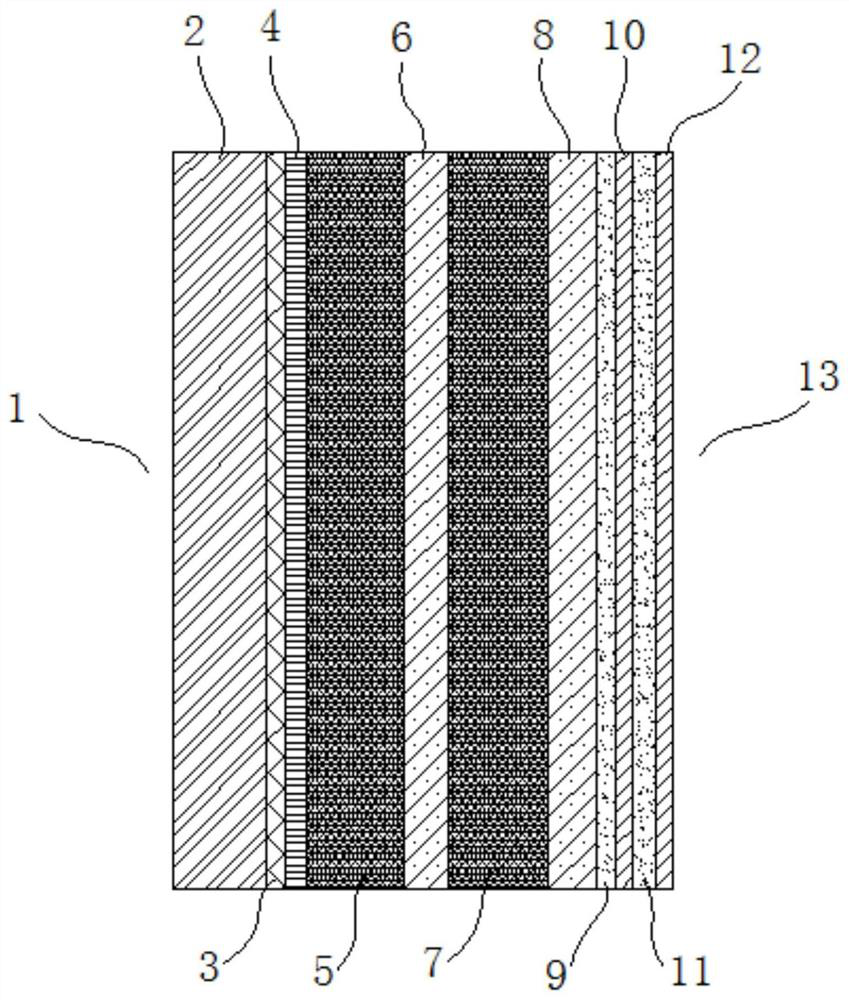
[0031] Such as image 3 As shown, the CO based on the SiC substrate 2 The reflective film includes a silicon carbide base layer, a diamond-like film layer, a nickel-chromium alloy adhesive layer, a metal film, a first germanium layer, a first zinc sulfide layer, a second germanium layer, a second zinc sulfide layer, The first YbF3 layer, the first ZnSe layer, the second YbF3 layer and the second ZnSe layer; the thickness of the diamond-like film layer is 1.2 μm, the thickness of the nickel-chromium alloy bonding layer is 0.2 μm, and the thickness of the metal film is 0.2 μm, The thickness of the first germanium layer is 1.7 μm, the thickness of the first zinc sulfide layer is 0.5 μm, the thickness of the second germanium layer is 1.7 μm, the thickness of the second zinc sulfide layer is 0.5 μm, and the thickness of the first YbF3 layer is 0.18 μm, the thickness of the first ZnSe layer is 0.08μm, the second YbF 3 The thickness of the layer is 0.18 μm and the thickness of the ...

Embodiment 2

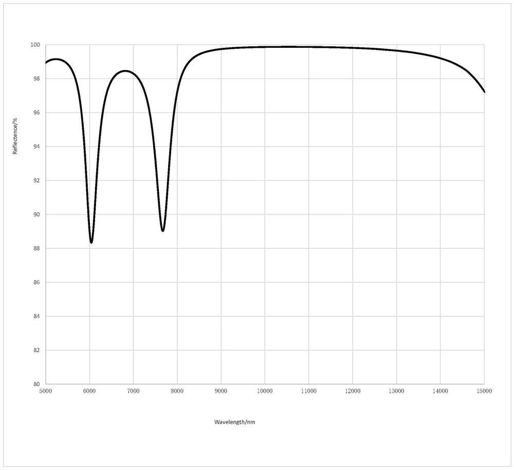
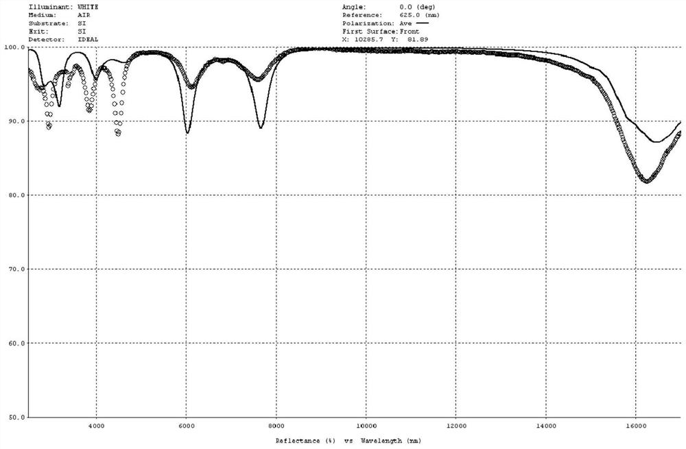
[0043] CO based on SiC substrates 2 Reflective film, the difference of embodiment 1 is: the thickness of the diamond-like film layer is 1.1 μm, the thickness of the nickel-chromium alloy bonding layer is 0.2 μm, the thickness of the metal film is 0.2 μm, and the thickness of the first germanium layer is 1.6 μm , the thickness of the first zinc sulfide layer is 0.6 μm, the thickness of the second germanium layer is 1.6 μm, the thickness of the second zinc sulfide layer is 0.6 μm, the thickness of the first YbF3 layer is 0.19 μm, and the thickness of the first ZnSe layer is 0.07μm, second YbF 3 The thickness of the layer is 0.19 μm and the thickness of the second ZnSe layer is 0.07 μm; the preparation method refers to Example 1; the infrared spectrophotometer Spectrum100 is used for index detection, and the single-sided reflection at 10600 nm reaches 99.8%, and the reflection at the red light reaches 80% ;


PUM

PropertyMeasurementUnit
thicknessaaaaaaaaaa
thicknessaaaaaaaaaa
thicknessaaaaaaaaaa

Abstract

The invention discloses a CO based on silicon carbide substrate 2 Reflective film and its preparation method, CO based on silicon carbide substrate 2 Reflective film, including sequentially connected silicon carbide base layer, diamond-like film layer, nickel-chromium alloy adhesive layer, metal film, more than one group of alternately arranged germanium layers and zinc sulfide layers, and more than one group of alternately arranged YbF 3 layer and ZnSe layer. The present invention is based on silicon carbide substrate CO 2 Reflective film, the film system has a reflection of 99.8% in the far infrared 10.6um band, and can withstand high temperatures of 300 degrees, low density, high elastic modulus, low thermal expansion coefficient, high thermal conductivity, strong adhesion, and temperature resistance Good resistance to heat and humidity, no thermal stress, uniform linear expansion coefficient, isotropic thermal and mechanical properties; simple preparation, easy to obtain raw materials, and low cost.

Description

technical field [0001] The present invention relates to a CO based on a silicon carbide substrate 2 A reflective film and a preparation method thereof belong to the field of reflective films on silicon carbide substrates. Background technique [0002] With the rapid development of science and technology, some advanced optical systems, such as reconnaissance systems, meteorological observation systems, etc., put forward higher and higher requirements for the performance of the reflector of the system itself. [0003] Silicon carbide has emerged in various silicon carbide mirror preparation processes due to its advantages of low cost and short production cycle. Due to its unique crystal structure, the surface of silicon carbide presents a honeycomb structure. Although the surface roughness of silicon carbide has reached within 0.02 microns, how to coat the film firmly on this lens and how to reduce the damage caused by the crystal structure on the surface of the lens The pro...

Claims


Application Information

Patent Timeline
Patent Type & Authority Patents(China)
IPC IPC(8): G02B5/08G02B1/10
CPCG02B1/10G02B5/0808
Inventor 李全民陈莉陈佳佳朱敏王国力吴玉堂
Owner NANJING WAVELENGTH OPTO ELECTRONICS SCI & TECH CO LTD
Why Eureka
Try Eureka