
MEMS micro hot plate based on air thermal insulation layer and manufacturing method of MEMS micro hot plate

A technology of air heat insulation layer and micro-hot plate, which is applied to the process, coating, and electrical components used to produce decorative surface effects, and can solve the problem of uneven temperature distribution of MEMS micro-hot plates, affecting the gas sensor characteristics of gas sensors, Problems such as high power of MEMS micro-hot plate, to achieve the effect of reducing loss, suppressing loss, and reducing power consumption

Active Publication Date: 2020-09-22
复微感知(合肥)科技有限公司
View PDF11 Cites 3 Cited by
  • Summary
  • Abstract
  • Description
  • Claims
  • Application Information

AI Technical Summary

Problems solved by technology

However, because the traditional MEMS micro-hotplate makes the heating electrode and the test electrode in different layers, the power of the MEMS micro-hotplate is high, and the temperature distribution on the MEMS micro-hotplate is uneven, that is, the central temperature of the MEMS micro-hotplate The temperature difference from the edge is very large, resulting in a large difference in the gas-sensing response of the gas-sensing film on the upper part of the MEMS micro-hot plate, which ultimately affects the gas-sensing characteristics of the entire gas sensor

Method used


Image

  • MEMS micro hot plate based on air thermal insulation layer and manufacturing method of MEMS micro hot plate
  • MEMS micro hot plate based on air thermal insulation layer and manufacturing method of MEMS micro hot plate
  • MEMS micro hot plate based on air thermal insulation layer and manufacturing method of MEMS micro hot plate

Examples


Embodiment 1

[0043] Embodiment 1: Making the thickness t of the air insulation layer a 0.5 μm, p-type (100) silicon chip thickness h is 200 μm MEMS micro-hot plate based on air insulation layer.

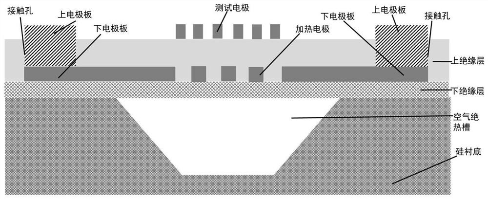
[0044] Step 1, making the lower insulating layer on the silicon substrate, such as Image 6 a.

[0045] On silicon substrates, using thermal oxidation technology, that is, in O 2 Under the technological conditions of flow rate of 20sccm, pressure of 20mT, and temperature of 500°C, a layer of thickness t d 1µm SiO 2 The insulating medium forms the lower insulating layer.

[0046] Step 2, making a sacrificial layer on the lower insulating layer, such as Image 6 b.

[0047] On the lower insulating layer, use chemical vapor deposition technology, that is, in the reaction chamber temperature of 1200 ° C, SiCl 4 Flow at H 2 The molar percentage in is 5%, and the film growth rate is 2.2μm / min under the process conditions, depositing a layer thickness t a 0.5μm polysilicon;

[0048] Use reacti...

Embodiment 2

[0063] Embodiment 2: Making the thickness t of the air insulation layer a 1 μm, p-type (100) silicon chip thickness h is 300 μm MEMS micro-hot plate based on air insulation layer.

[0064] Step 1, making a lower insulating layer on the silicon substrate, such as Image 6 a.

[0065] A layer of thickness t is grown on a silicon substrate by thermal oxidation d 2µm SiO 2 The insulating medium forms the lower insulating layer.

[0066] The processing condition of described thermal oxidation technology is: O 2 The flow rate is 30 sccm, the pressure is 80 mT, and the temperature is 550°C.

[0067] Step 2, making a sacrificial layer, such as Image 6 b.

[0068] 2.1) Deposit a layer thickness t on the lower insulating layer by using chemical vapor deposition technology a 1μm polysilicon;

[0069] 2.2) A mask is made on the surface of the polysilicon, and the easily corroded material layer is etched into a rectangular parallelepiped sacrificial layer by reactive ion etching ...

Embodiment 3

[0091] Embodiment three: making air heat insulation layer thickness t a 2μm, p-type (100) silicon chip thickness h is 500μm MEMS micro hot plate based on air insulation layer.

[0092] Step A, making a lower insulating layer on the silicon substrate, such as Image 6 a.

[0093] Using thermal oxidation technology in O 2 The flow rate is 40 sccm, the pressure is 100mT, and the temperature is 600°C, a layer of thickness t is grown on the silicon substrate d 5µm SiO 2 The insulating medium forms the lower insulating layer.

[0094] Step B, making a sacrificial layer on the lower insulating layer, such as Image 6 b.

[0095] First, using chemical vapor deposition technology in the reaction chamber temperature of 1200 ° C, SiCl 4 Flow at H 2 Deposit a layer of thickness t on the lower insulating layer under the condition that the molar percentage in the film is 5%, and the film growth rate is 2.2 μm / min. a 2μm polysilicon;

[0096] Then, make a mask on the surface of the...


PUM

PropertyMeasurementUnit
thicknessaaaaaaaaaa
thicknessaaaaaaaaaa
thicknessaaaaaaaaaa

Abstract

The invention discloses an MEMS micro hot plate based on an air thermal insulation layer and a manufacturing method of the MEMS micro hot plate, and mainly solves the problems of uneven temperature distribution and high power consumption of the existing micro hot plate. The MEMS micro hot plate comprises a silicon substrate (1), a lower insulating layer (2), an upper insulating layer (3) and a covering layer (4) from bottom to top, wherein a test electrode (5) and a heating electrode (6) are arranged in the middle of the upper part of the covering layer (4); the test electrode (5) is surrounded by a heating electrode (6), polar plates (7) are arranged at four diagonal positions of the upper part of the covering layer (4); the silicon substrate (1) is corroded to form an air heat insulationgroove (8); a through hole array (10) and an air heat insulation layer (9) are arranged in the middle of the upper insulating layer (3) from top to bottom, the lower insulating layer (2), the upper insulating layer (3) and the covering layer (4) form a heating platform (11) and a cantilever (12) at the same time through corrosion. The MEMS micro hot plate is uniform in temperature distribution, low in power consumption and capable of being used for gas sensors.

Description

[0001] The invention belongs to the technical field of microelectronic devices, and in particular relates to a MEMS micro-hot plate and a manufacturing method thereof, which can be used as a heating device in a gas sensor. [0002] technical background [0003] At present, micro-electromechanical system MEMS gas sensors play an extremely important role in the fields of artificial intelligence, Internet of Things, air quality monitoring, chemical production, and safe home due to their high sensitivity, low power consumption, small size, and easy integration. . MEMS gas sensors are usually composed of two parts: a MEMS micro-hot plate and a gas-sensitive membrane. The MEMS micro-hot plate plays a vital role in providing a stable and constant operating temperature to ensure that the gas-sensitive membrane can accurately detect For the change of measured gas concentration, see Zhao Ruru, MEMS Integrated Formaldehyde Sensor Design and Performance Testing Research, Harbin University ...

Claims


Application Information

Patent Timeline
Patent Type & Authority Applications(China)
IPC IPC(8): G01N27/12H05B3/20B81C1/00B81B7/02
CPCB81B7/02B81C1/00015G01N27/128H05B3/20
Inventor 杨翠毛维闵星艾治州史芝纲王晓飞
Owner 复微感知(合肥)科技有限公司
Features
  • Generate Ideas
  • Intellectual Property
  • Life Sciences
  • Materials
  • Tech Scout
  • Unparalleled Data Quality
  • Higher Quality Content
  • 60% Fewer Hallucinations
Learn More