Communication optical amplifier and photodiode detector integrated component and preparation method

A photodiode and integrated component technology, applied in radiation control devices and other directions, can solve the problems of increasing the complexity of semiconductor epitaxy technology, loss, development cost and technical limitations, etc., to reduce the accuracy of epitaxy process requirements, easy to achieve, easy to achieve control effect

Active Publication Date: 2021-06-25
SHANXI YUANJIE SEMICONDUCTOR TECH CO LTD
View PDF6 Cites 0 Cited by
  • Summary
  • Abstract
  • Description
  • Claims
  • Application Information

AI Technical Summary

Problems solved by technology

[0004] The current solution at home and abroad is to integrate SOA on the laser at the transmitting end to increase the optical power at the transmitting end to meet the high sensitivity requirements at the receiving end. This solution causes the integrated SOA laser at the transmitting end to be only compatible with a very small number of large manufacturers in the United States and Japan. According to the discussion, due to the high price and the constraints of the manufacturer, the 50G PON system that was originally expected to use the generally mature 25G optical device plus PAM4 modulation technology has become extremely high in development costs and technology restrictions, and has lost its original meaning.
[0005] In order to solve this problem, SOA (optical amplifier) ​​and PIN (photodiode) integrated technology detector elements can be used. Generally speaking, the incident light is introduced into the detector to reduce the coupling loss, and the detector has a large light receiving area. Optical cavity design, so SOA (optical amplifier) ​​and PIN (photodiode) integrated components must also adopt a vertical optical cavity design with a large light-receiving area, but this method will increase the complexity of semiconductor epitaxy technology, and each layer in the epitaxial layer The design and process control of the design and process control need to have a certain precision, which raises the technical threshold of mass production

Method used


Image

  • Communication optical amplifier and photodiode detector integrated component and preparation method
  • Communication optical amplifier and photodiode detector integrated component and preparation method
  • Communication optical amplifier and photodiode detector integrated component and preparation method

Examples


Embodiment 1

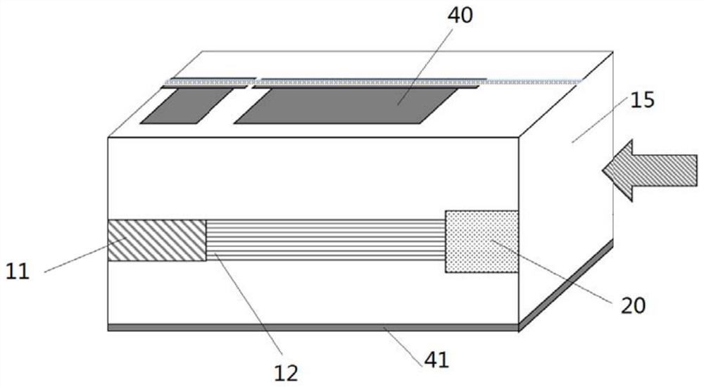
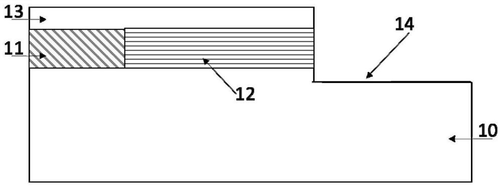
[0057] In this embodiment, the etching depth (that is, the height difference between the etched bottom surface of the end face etching region 14 and the bottom surface of the optical amplifier active layer 12) T1 and the thickness T2 of the pattern converter structure layer are optimally designed. Regarding the pattern converter region The optimization of the waveguide length Lssc and the waveguide width W2 at the light-receiving end of the mode-spot converter will be optimized and designed item by item in Embodiments 2 and 3, respectively. Therefore, in Example 1, the waveguide length Lssc in the mode spot converter area and the waveguide width W2 at the receiving end of the mode spot converter will first take the middle value of the value range (that is, Lssc=35um and W2=6.5um), and so on The value optimizes the etching depth T1; the optimization result is as follows Figure 4a As shown, when the thickness T2 of the pattern converter structure layer reaches 500nm, the improv...

Embodiment 2

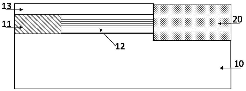
[0059]In order to optimize the design of the waveguide length Lssc in the speckle converter area in this embodiment, the optimum etching depth T1=150nm in Example 1 and the optimized structural layer thickness of the speckle converter T2=500nm are taken as the design premise, and the speckle conversion The waveguide width W2 at the receiving end of the receiver is taken as the middle value of the value range (W2=6.5um); Figure 4b As shown, the coupling loss is measured when the waveguide length Lssc in the mode spot converter area is 20 um -50 um. In the mode spot converter area, the waveguide length Lssc=45um has the lowest coupling loss value of 4.9dB, so the length is The optimal waveguide length and the coupling loss can be improved by 0.6dB compared with Lssc=35um in the original embodiment 1.

Embodiment 3

[0061] This embodiment is to optimize the waveguide width W2 at the light-receiving end of the speckle converter. The optimal etching depth T1=150nm in Examples 1 and 2 is used, and the structural layer thickness of the speckle converter after optimization is T2=500nm and the optimum speckle The waveguide length Lssc=45um in the converter area is the design premise. Such as Figure 4c As shown, when the waveguide width W2=8um at the receiving end of the mode-spot converter, the coupling loss has approached the saturation value, and can reach an extremely low loss level less than 4dB. The improvement of W2 width is limited, considering the process production. High uniformity of the waveguide width is conducive to the premise of production control, so W2=8um is the optimal waveguide length, and the coupling loss can be improved by 0.95dB compared with the design of W2=6.5um in the original embodiment 2, and the final coupling loss value It can reach 3.95dB, and this coupling lo...


PUM

PropertyMeasurementUnit
thicknessaaaaaaaaaa
thicknessaaaaaaaaaa

Abstract

The invention discloses an integrated component of an optical amplifier for communication and a photodiode detector and a preparation method thereof. The integrated component includes a substrate on which a photodiode active layer, an optical amplifier active layer, and a mode spot converter structure layer are sequentially arranged. The converter structure layer is located close to the light-receiving end face of the integrated element, the bottom surface of the mode spot converter structure layer is lower than the bottom surface of the optical amplifier active layer, and the photodiode active layer and the optical amplifier active layer are covered with a first cladding layer , the first cladding layer and the pattern converter structure layer are covered with a second cladding layer, the second cladding layer is covered with a contact layer and a p-metal electrode layer in sequence from bottom to top, and the lower surface of the substrate is plated with an n-metal electrode layer . The invention uses the mottled converter as a semiconductor optical waveguide structure to improve the coupling efficiency; adopts the form of edge coupling to introduce the incident light into the integrated detector element, simplifies the process flow, and can realize the domestic production of the optical detector at the receiving end of the system above 50G PON mass production.

Description

technical field [0001] The invention belongs to the technical field of semiconductor optical detectors for communication, and in particular relates to an integrated component of an optical amplifier and a photodiode detector for communication and a preparation method. Background technique [0002] With the increase of the capacity demand of the communication network, the existing 10G PON network needs to further increase the system bandwidth to meet the demand of the future market. In the next stage of system bandwidth improvement, it is expected that 25G PON, 50G PON and even 100G PON higher-speed systems will be considered; the improvement schemes of these systems are mainly based on the use of more mature 25G devices. Compared with 10G PON, we are committed to developing The difficulty of 25G PON is the lowest, but due to the small increase in speed, it will still face speed bottlenecks in the future. Therefore, the development of systems above 50G PON has been started by...

Claims


Application Information

Patent Timeline
Patent Type & Authority Patents(China)
IPC IPC(8): H01L27/144
CPCH01L27/144
Inventor 潘彦廷李马惠陈发涛曹凡穆瑶
Owner SHANXI YUANJIE SEMICONDUCTOR TECH CO LTD
Why Eureka
Try Eureka