Organic photoelectric material, preparation method and application thereof

An organic optoelectronic material, an unreplaced technology, applied in the field of organic electroluminescence, which can solve the problems of high cost, many steps of axenic compounds, and poor stability of metal complexes

Pending Publication Date: 2020-10-27
EVERDISPLAY OPTRONICS (SHANGHAI) CO LTD
View PDF8 Cites 1 Cited by
  • Summary
  • Abstract
  • Description
  • Claims
  • Application Information

AI Technical Summary

Problems solved by technology

[0007] However, in the prior art, the host materials of hole injection materials are mostly aromatic amine compounds, and the dopant materials of the doped hole injection layer are mostly Lewis acid metal

Method used


Image

  • Organic photoelectric material, preparation method and application thereof
  • Organic photoelectric material, preparation method and application thereof
  • Organic photoelectric material, preparation method and application thereof

Examples


Embodiment 1

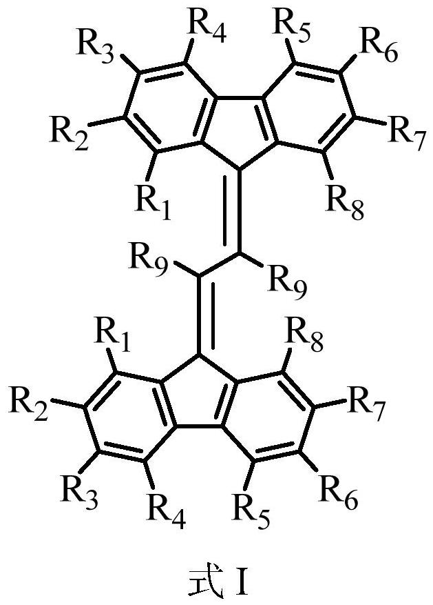
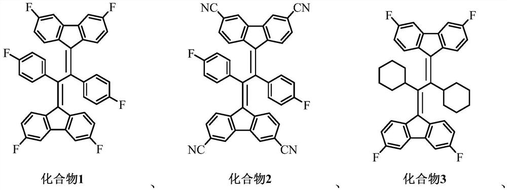
[0063] This embodiment provides an organic optoelectronic material compound 1, the structural formula of compound 1 is as follows The reaction formula for preparing compound 1 is:

[0064]

[0065] Concrete preparation method comprises the following steps:

[0066] (1) Add 2.17g of compound 1a (5mmol), 30mL of n-heptane and 20mL of diethyl ether into a Schelenk tube with nitrogen and oxygen isolation, and cool the solution to -78°C; then add 8.5mL, 1.3mol / L tert-butyllithium solution (solvent is n-heptane), stirred at -78°C for 8 minutes; removed the ice bath, and continued to stir for 15 minutes to obtain a reaction intermediate;

[0067] (2) 40.5mg FeCl 3 (0.25mmol) was dissolved in 2.5mL tetrahydrofuran to obtain a mixed solution, which was added to the reaction intermediate obtained in step (1); then di-tert-butyl peroxide (DTBP, 0.91mL, 5.0mmol) was added, and after stirring for 30min The reaction temperature was adjusted to room temperature, and the entire reacti...

Embodiment 2

[0071] This embodiment provides an organic optoelectronic material compound 2, the structural formula of compound 2 is as follows The reaction formula for preparing compound 2 is:

[0072]

[0073] Concrete preparation method comprises the following steps:

[0074] (1) Add 2.34g of compound 2a (5mmol), 30mL of n-heptane and 20mL of diethyl ether into a Schelenk tube with nitrogen to isolate oxygen, and cool the solution to -78°C; then add 8.5mL and 1.3mol of / L tert-butyllithium solution (solvent is n-heptane), stirred at -78°C for 8 minutes; removed the ice bath, and continued to stir for 15 minutes to obtain a reaction intermediate;

[0075] (2) 40.5mg FeCl 3(0.25mmol) was dissolved in 2.5mL tetrahydrofuran to obtain a mixed solution, which was added to the reaction intermediate obtained in step (1); then di-tert-butyl peroxide (DTBP, 0.91mL, 5.0mmol) was added, and after stirring for 30min The reaction temperature was adjusted to room temperature, and the entire reac...

Embodiment 3

[0079] This embodiment provides an organic optoelectronic material compound 3, the structural formula of compound 3 is as follows The reaction formula for preparing compound 3 is:

[0080]

[0081] Concrete preparation method comprises the following steps:

[0082] (1) Add 2.20g of compound 3a (5mmol), 30mL of n-heptane and 20mL of diethyl ether into a Schelenk tube with nitrogen to isolate oxygen, and cool the solution to -78°C; then add 8.5mL and 1.3mol of / L tert-butyllithium solution (solvent is n-heptane), stirred at -78°C for 8 minutes; removed the ice bath, and continued to stir for 15 minutes to obtain a reaction intermediate;

[0083] (2) 40.5mg FeCl 3 (0.25mmol) was dissolved in 2.5mL tetrahydrofuran to obtain a mixed solution, which was added to the reaction intermediate obtained in step (1); then di-tert-butyl peroxide (DTBP, 0.91mL, 5.0mmol) was added, and after stirring for 30min The reaction temperature was adjusted to room temperature, and the entire rea...


PUM

PropertyMeasurementUnit
Nmraaaaaaaaaa

Abstract

The invention provides an organic photoelectric material, which has a structure represented by a formula I. According to the invention, the organic photoelectric material contains a substituted butadiene skeleton structure, and two double bonds form a conjugated system, so that the thermal stability of the material is improved, and the film-forming property of the organic photoelectric material inthe processing process is further improved; under the combined action of the cross conjugate structure in the molecule and the electron withdrawing group in the substituent group, the molecule has high reduction potential so as to assist the hole transport layer to perform efficient hole injection; and the organic photoelectric material is used as a hole injection layer object material of an OLEDdevice, so that charge injection can be effectively increased, the driving voltage of the OLED device is reduced, the service life of the device is prolonged, and the overall efficiency of the deviceis improved.

Description

technical field [0001] The invention belongs to the technical field of organic electroluminescence, and specifically relates to an organic photoelectric material and its preparation method and application. Background technique [0002] With the development of organic electronics, organic electroluminescent devices (OLEDs) have rapidly become a research hotspot, and have great potential to replace mainstream liquid crystal displays and become a star technology in the display field. The growing demand in the display field has also led to the rapid development of OLED device structures and organic photoelectric materials, specifically manifested in the emergence of compounds and materials with new structures, functional groups and substituents, and the continuous optimization of OLED device structures. The sandwich structure has gradually developed into a complex structure composed of multiple functional layers. [0003] In the design of OLED devices, energy level matching is ...

Claims


Application Information

Patent Timeline
IPC IPC(8): C07C25/24C07C255/52C07C255/51C07C253/30C07C17/269C09K11/06H01L51/50H01L51/54
CPCC07C25/24C07C255/52C07C255/51C09K11/06C09K2211/1007C09K2211/1011C07C2601/14C07C2603/18H10K85/626H10K85/615H10K50/15H10K50/00
Inventor 俞云海谭奇张晓龙
Owner EVERDISPLAY OPTRONICS (SHANGHAI) CO LTD
Why Eureka
Try Eureka