Eureka AIR delivers breakthrough ideas for toughest innovation challenges, trusted by R&D personnel around the world.

Enhanced high electron mobility transistor and manufacturing method thereof

A high electron mobility, transistor technology, applied in the field of microelectronics, can solve the problems of lower device yield, high manufacturing cost, cumbersome process debugging, etc.

Active Publication Date: 2020-10-27
XIDIAN UNIV
View PDF6 Cites 0 Cited by
  • Summary
  • Abstract
  • Description
  • Claims
  • Application Information

AI Technical Summary

Problems solved by technology

However, the process of source-drain compound double-layer field plate power switching device is complicated, and the manufacturing cost is higher. The fabrication of each field plate requires process steps such as photolithography, metal deposition, and passivation medium deposition.
Moreover, in order to optimize the thickness of the dielectric material under the field plates of each layer to maximize the breakdown voltage, tedious process debugging and optimization must be carried out, which greatly increases the difficulty of device manufacturing and reduces the yield of devices.

Method used

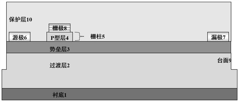

Image

  • Enhanced high electron mobility transistor and manufacturing method thereof
  • Enhanced high electron mobility transistor and manufacturing method thereof
  • Enhanced high electron mobility transistor and manufacturing method thereof

Examples


Embodiment 1

[0083] Embodiment 1: The thickness h of the P-type layer 6 is 20 nm, and the doping concentration of the P-type layer 6 is 5×10 20 cm -3 , N-type column 8 depth y 1 10nm, doping concentration is 5×10 20 cm -3 , the number of N columns 81 is 1, the length of grid columns 9 is 4nm, the array hole 10 is composed of 2×2 holes of the same size, the number of grooves is 3, and the number of independent metal blocks is 1. type high electron mobility transistors.

[0084] Step 1. Epitaxial GaN material is made transition layer 2 on sapphire substrate 1, as Figure 7 a.

[0085] 1a) GaN material with a thickness of 30nm was epitaxially grown on the sapphire substrate 1 by metal-organic chemical vapor deposition technology. The source flow rate is 22μmol / min;

[0086] 1b) GaN material with a thickness of 0.97 μm is epitaxially grown on the GaN material by metal-organic chemical vapor deposition technology to form an undoped transition layer 2. The process conditions are as follow...

Embodiment 2

[0130] Embodiment 2: The thickness h of making the P-type layer 6 is 200nm, and the doping concentration of the P-type layer 6 is 1×10 19 cm -3 , N-type column 8 depth y 1 80nm, the concentration is 5×10 19 cm -3 , the number of N columns 81 is 3, the length of grid columns 9 is 1800nm, the array hole 10 is composed of 5×5 holes of the same size, the number of grooves is 5, and the number of independent metal blocks is 3. type high electron mobility transistors.

[0131] Step 1. Epitaxially AlN and GaN materials on the silicon carbide substrate 1 to form the transition layer 2, such as Figure 7 a.

[0132] 1.1) Metal-organic chemical vapor deposition technology is used at a temperature of 1000° C., a pressure of 45 Torr, a hydrogen flow rate of 4600 sccm, an ammonia gas flow rate of 4600 sccm, and an aluminum source flow rate of 5 μmol / min, on a silicon carbide substrate 1 Undoped AlN material with an epitaxial thickness of 100nm;

[0133] 1.2) Using metal-organic chem...

Embodiment 3

[0163] Embodiment 3: The thickness h of the P-type layer 6 is 300 nm, and the doping concentration of the P-type layer 6 is 1×10 16 cm -3 , N-type column 8 depth y 1 250nm, doping concentration is 1×10 16 cm -3 , the number of N columns 81 is 5, the length of grid columns 9 is 5000nm, the array hole 10 is composed of 10×10 holes of the same size, the number of grooves is 7, and the number of independent metal blocks is 5. type high electron mobility transistors.

[0164] Step A. Epitaxial AlN and GaN materials on the silicon substrate 1 from bottom to top to make the transition layer 2, such as Figure 7 a.

[0165] First, AlN material with a thickness of 400nm is epitaxially grown on silicon substrate 1 by metal-organic chemical vapor deposition technology. The process condition that the source flow is 25μmol / min;

[0166] Then, use metal organic chemical vapor deposition technology to epitaxially GaN material with a thickness of 9.6 μm on the AlN material to complete ...


PUM

PropertyMeasurementUnit
Lengthaaaaaaaaaa
Doping concentrationaaaaaaaaaa
Work functionaaaaaaaaaa

Abstract

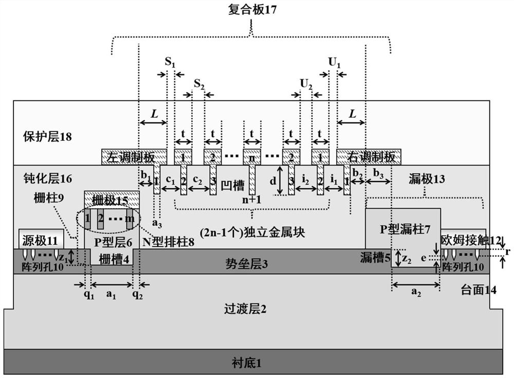
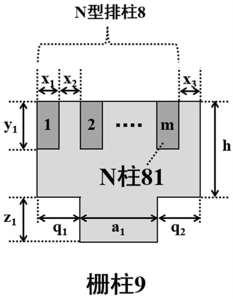
The invention discloses an enhanced high electron mobility transistor and a manufacturing method thereof. The objective of the invention is to solve the problems that an existing power switch device is low in threshold voltage and complex in process when high breakdown voltage is achieved. The transistor comprises a substrate (1), a transition layer (2), a barrier layer (3), a gate groove (4), a drain groove (5), a P-type layer (6), a P-type drain column (7), a gate column (9), a source (11), a table top (14), a grid electrode (15) and a passivation layer (16) N-type row columns (8) are arranged in the grid columns; array holes (10) are formed in the barrier layer on the left side of the gate column and the barrier layer on the right side of the P-type drain column; an ohmic contact (12) is arranged on the right side of the P-type drain column, and the P-type drain column and the ohmic contact jointly form a drain electrode (13); a composite plate (17) is arranged at the upper part ofthe passivation layer; and a protective layer (18) is arranged on the peripheries of the passivation layer and the composite board. The transistor is simple in process, good in forward blocking and reverse blocking and high in threshold voltage, and can be used as a switching device.

Description

technical field [0001] The invention belongs to the technical field of microelectronics, in particular to a power switching device, which can be used as a basic device of a power electronic system. [0002] technical background [0003] Power electronic systems are widely used in many fields such as aerospace, industrial equipment, electric vehicles, and household appliances. As an important component of power electronic systems, power switching devices are important tools for energy conversion and control. Therefore, the performance and reliability of power switching devices have a decisive impact on the technical indicators and performance of the entire power electronic system. At present, the performance of Si-based power switching devices has approached its theoretical limit, which cannot meet the requirements of high temperature, high voltage, high frequency, high efficiency and high power density of the next generation power electronic system. The third-generation wide...

Claims


Application Information

Patent Timeline
IPC IPC(8): H01L29/778H01L21/335H01L29/06H01L29/423
CPCH01L29/0611H01L29/0684H01L29/42316H01L29/66462H01L29/778
Inventor 毛维高北鸾马佩军杜鸣张春福张金风周弘刘志宏张进成郝跃
Owner XIDIAN UNIV
Why Eureka
Eureka Blog
Learn More