
Micro-LED chip with epitaxial growth in selected area and preparation method of Micro-LED chip

A selective area epitaxy and chip technology, applied in identification devices, instruments, semiconductor devices, etc., can solve the problems of small improvement, lowering the electrical injection efficiency of p-GaN layer, and the influence of the electrical performance of Micro-LED chips, to prevent crosstalk, improve Display effect, improve the effect of photoelectric performance

Inactive Publication Date: 2020-10-30
WUHAN UNIV
View PDF2 Cites 6 Cited by
  • Summary
  • Abstract
  • Description
  • Claims
  • Application Information

AI Technical Summary

Problems solved by technology

Although sidewall passivation can reduce plasma damage during dry etching to a certain extent, even if more advanced atomic layer deposition (ALD) is used to replace standard plasma-enhanced chemical vapor deposition (PECVD) technology, this improvement is also smaller
In addition, the electrical injection efficiency of the p-GaN layer will be reduced during the passivation process, which will have a new impact on the electrical performance of the Micro-LED chip

Method used


Image

  • Micro-LED chip with epitaxial growth in selected area and preparation method of Micro-LED chip
  • Micro-LED chip with epitaxial growth in selected area and preparation method of Micro-LED chip
  • Micro-LED chip with epitaxial growth in selected area and preparation method of Micro-LED chip

Examples


Embodiment 1

[0045] A method for preparing a Micro-LED chip grown by selective epitaxial growth is provided, which specifically includes the following steps:

[0046] 1) Provide a sapphire substrate with a thickness of 400 μm, and then grow an n-GaN layer 1 with a thickness of 2.5 μm on the sapphire substrate 1 by MOCVD technology;

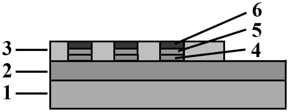
[0047] 2) Deposit SiO on the n-GaN layer 1 obtained in step 1) by PECVD 2 insulating dielectric layer with a thickness of 500nm, such as figure 1 shown;

[0048]3) after preparing a mask layer on the insulating dielectric layer obtained in step 2) by using photolithography technology, using ICP etching technology to selectively etch the insulating dielectric layer to obtain a microhole array penetrating through the insulating dielectric layer, and The n-GaN layer 1 is exposed at the edge of one side of the insulating medium layer to obtain a mesa structure of the n-GaN layer 1, wherein the microporous structure is a regular hexagonal prism with a bottom side...


PUM

PropertyMeasurementUnit
thicknessaaaaaaaaaa
thicknessaaaaaaaaaa
thicknessaaaaaaaaaa

Abstract

The invention discloses an epitaxial growth Micro-LED chip in a selected area and a preparation method of the epitaxial growth Micro-LED chip. The chip of a flip chip structure comprises a substrate,an n-GaN layer, an insulating dielectric layer and an ITO transparent conductive layer sequentially arranged from top to bottom. The insulating dielectric layer is provided with a chip epitaxial layerarray penetrating through the insulating dielectric layer, the n-GaN layer is exposed at the edge of one side of the insulating dielectric layer to form a mesa structure, the surface of the insulating dielectric layer is provided with an n electrode, the surface of the ITO transparent conductive layer is provided with a p electrode, and the p electrode and the n electrode are fixedly connected with a target substrate. In the preparation process, selective etching is carried out on the insulating dielectric layer to obtain a micropore array, and an epitaxial layer structure of the Micro-LED chip grows in micropores. According to the method, surface damage caused in the dry etching process of the epitaxial structure of the Micro-LED chip can be avoided, the Micro-LEDs are isolated from oneanother through the insulating dielectric layers, crosstalk can be prevented, and the display effect is improved.

Description

technical field [0001] The invention relates to the technical field of semiconductor light emitting diodes, in particular, the invention relates to an area-selective epitaxial growth Micro-LED chip and a preparation method thereof. Background technique [0002] Due to the advantages of small size, high resolution, low energy consumption, and high reliability, Micro-LED has great application value in high-resolution display, augmented reality, virtual reality, wearable electronics and other fields. Usually, the chip size of Micro-LED is less than 100 μm, and in the fields of virtual reality and augmented reality, its size is required to be as small as less than 5 μm. At present, for group III nitride Micro-LEDs, it is usually prepared by a combination of standard photolithography and dry etching. However, the process of dry etching the epitaxial structure will inevitably cause surface damage to the Micro-LED chip, which increases the surface non-radiative recombination rate ...

Claims


Application Information

Patent Timeline
Patent Type & Authority Applications(China)
IPC IPC(8): H01L33/32H01L33/08H01L33/06H01L33/36H01L33/00H01L27/15G09F9/33
CPCG09F9/33H01L27/156H01L33/0066H01L33/0075H01L33/06H01L33/08H01L33/32H01L33/36
Inventor 周圣军缪佳豪
Owner WUHAN UNIV
Learn More