Preparation method of storage bit and preparation method of MRAM

A storage bit and magnetic tunnel junction technology, applied in the field of semiconductor memory chip manufacturing, can solve problems such as magnetic damage

Pending Publication Date: 2020-10-30
ZHEJIANG HIKSTOR TECHOGY CO LTD
View PDF16 Cites 1 Cited by
  • Summary
  • Abstract
  • Description
  • Claims
  • Application Information

AI Technical Summary

Problems solved by technology

[0007] The main purpose of the present invention is to provide a preparation method of storage bits and a preparati

Method used


Image

  • Preparation method of storage bit and preparation method of MRAM
  • Preparation method of storage bit and preparation method of MRAM
  • Preparation method of storage bit and preparation method of MRAM

Examples


preparation example Construction

[0031] As introduced in the background art, the manufacturing process of storage bits in the prior art easily leads to magnetic damage of the device. In order to solve the above-mentioned technical problems, the applicant of the present invention provides a method for preparing a storage bit, including the step of forming a magnetic tunnel junction. After the step of forming a magnetic tunnel junction, the preparation method further includes the following steps: The junction sidewalls are gas passivated to reduce dangling bonds on their sidewall surfaces.

[0032] No matter what etching method is adopted, a large number of high-energy particles will irradiate the tunnel junction during etching, resulting in not only uneven surface and large specific surface area of ​​the etched tunnel junction, but also chaotic surface lattice, dislocations, impurities, The vacancy density is high, the magnetic anisotropy of the surface area is not strong, and multi-domain inversion is prone t...

Embodiment 1

[0053] The method for preparing storage bits provided in this embodiment includes the following steps:

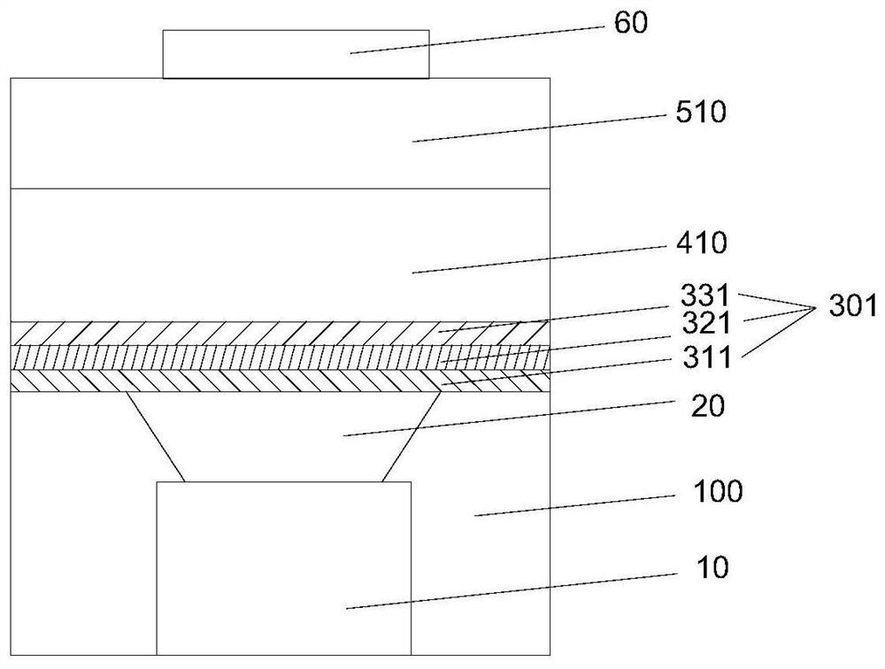
[0054] The second mask material layer 510 is deposited on the first mask material layer 410, and the photoresist 60 is covered on the second mask material layer 510, and the photoresist 60 is patterned by photolithography and developing processes, so as to The photoresist 60 is used as a mask to etch the second mask material layer 510 to obtain the second mask layer 50 with the same pattern as the photoresist 60, such as figure 1 with figure 2 shown; then through the second mask layer 50, the first mask material layer 410 is etched to transfer the pattern of the patterned photoresist 60 to obtain the first mask layer 40;

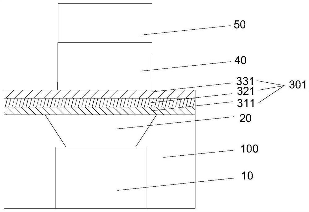
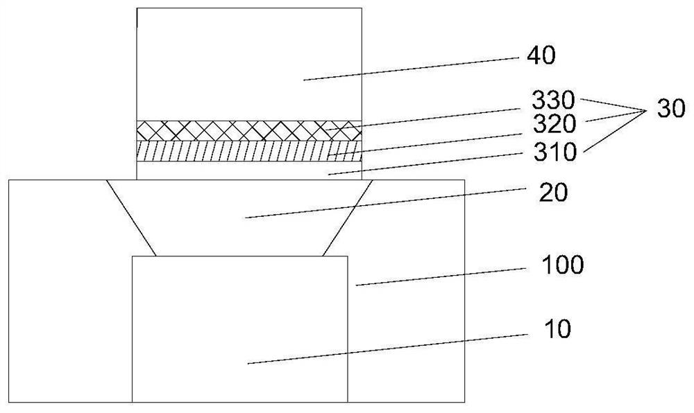
[0055] The tunnel junction material layer 301 is etched through the first mask layer 40 to form a magnetic tunnel junction 30, including a reference layer 310, a barrier layer 320 and a free layer 330, and the etching stays below the bottom electrode 20...

Embodiment 2

[0059] The difference between the method for preparing storage bits provided in this embodiment and that of Embodiment 1 is that:

[0060] The hydrogen flow rate is 10 sccm, the argon gas flow rate is 5000 sccm, the air pressure is 1 Torr, the power is 10 W, the temperature is 20° C., and the processing time is 500 s.


PUM

PropertyMeasurementUnit
Thicknessaaaaaaaaaa

Abstract

The invention provides a preparation method of a storage bit and a preparation method of an MRAM. The preparation method comprises step of forming the magnetic tunnel junction, and after the step of forming the magnetic tunnel junction, the preparation method further comprises the following step of performing gas passivation treatment on the side wall of the magnetic tunnel junction to reduce dangling bonds on the surface of the side wall. According to the preparation method, passivation treatment is carried out through the gas, dangling keys on a surface of a side wall can be reduced, surfaceimpurities can be removed, and vacancies in the surface layer and on the surface can be filled, so defect density is reduced, device stability is improved, influence of etching damage on performanceparameters such as TMR is relieved, the TMR loss reduction rate, the TMR discrete value and the critical voltage discrete value of the device array can be reduced, and the critical magnetic field is improved.

Description

technical field [0001] The invention relates to the field of manufacturing semiconductor memory chips, in particular to a method for preparing a storage bit and a method for preparing an MRAM. Background technique [0002] Memory chips are an important part of computers, affecting the speed, integration and power consumption of the entire computer. Inside the current computer, the memory is divided into two parts, the hard disk and the cache. The hard disk has a large capacity, and the data will not be lost when the power is turned off, but the speed is slow. Even the more advanced SSD NAND Flash cannot be avoided. The cache speed is fast, such as DRAM and SRAM, but the capacity is small, and the data is lost when the power is off. With the gradual reduction of chip feature size, NAND, DRAM and SRAM face a series of insurmountable difficulties such as large power consumption and large area. [0003] MRAM is currently the most promising next-generation memory chip. It co...

Claims


Application Information

Patent Timeline
IPC IPC(8): H01L43/08H01L43/14G11C11/16
CPCG11C11/161H10N52/01H10N50/10
Inventor 王曙光李辉辉
Owner ZHEJIANG HIKSTOR TECHOGY CO LTD
Why Eureka
Try Eureka