
Silicon nitride assisted lithium niobate thin film waveguide-based full-integrated optical transceiving system

A thin-film waveguide and transceiver system technology, applied in the field of integrated optics, can solve the problems of increased difficulty in device design, difficulty in having smooth boundaries in waveguide structures, difficulty in monolithic full integration of optical communication system functional devices, etc., to reduce production costs, The effect of reducing process difficulty and expanding communication capacity

Inactive Publication Date: 2020-11-03
LANZHOU UNIVERSITY
View PDF13 Cites 4 Cited by
  • Summary
  • Abstract
  • Description
  • Claims
  • Application Information

AI Technical Summary

Problems solved by technology

At present, the most common method to realize lithium niobate thin-film waveguide is still direct etching, but the waveguide structure formed by direct etching is difficult to have smooth boundaries. In addition, in the design of some devices sensitive to waveguide parameters In the design process, the chamfer that may be formed by etching must be strictly taken into account, which increases the difficulty of device design.
To sum up, whether it is based on silicon waveguide or lithium niobate thin film waveguide, it is difficult to complete the monolithic full integration of the main functional devices in the optical communication system through the existing technical means

Method used


Image

  • Silicon nitride assisted lithium niobate thin film waveguide-based full-integrated optical transceiving system
  • Silicon nitride assisted lithium niobate thin film waveguide-based full-integrated optical transceiving system
  • Silicon nitride assisted lithium niobate thin film waveguide-based full-integrated optical transceiving system

Examples


Embodiment Construction

[0015] The present invention will be described in detail below in conjunction with the accompanying drawings and specific embodiments.

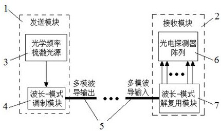
[0016] Such as figure 1 As shown, the optical transceiver system of the present invention includes a sending module 1 and a receiving module 2 , and the sending module 1 and the receiving module 2 are connected through a multimode waveguide 5 .

[0017] The sending module 1 includes a connected optical frequency comb laser source 3 and a wavelength-mode modulation module 4 .

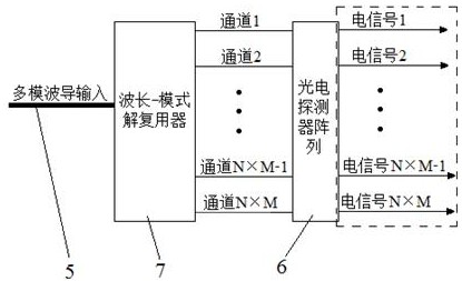
[0018] The receiving module 2 includes a connected photodetector array 6 and a wavelength-mode demultiplexing module 7, such as figure 2 shown.

[0019] The wavelength-mode modulation module 4 is connected to the wavelength-mode demultiplexing module 7 through a multimode waveguide 5 .

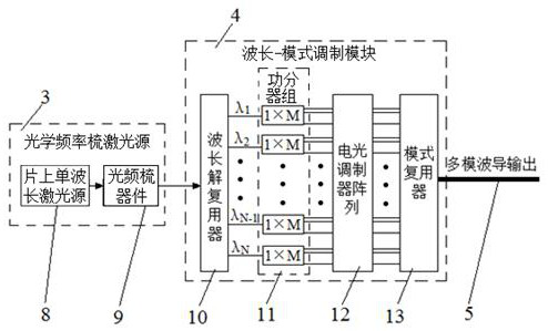
[0020] The optical frequency comb laser source 3 in the sending module 1 includes a connected on-chip single-wavelength laser source 8 and an optical frequency comb device 9; the wa...


PUM


Abstract

The invention provides a silicon nitride assisted lithium niobate thin film waveguide-based full-integrated optical transceiving system. The system comprises a transmitting module and a receiving module which are connected through a multimode waveguide, the optical frequency comb laser source comprises an on-chip single-wavelength laser source and an optical frequency comb device which are connected. The wavelength-mode modulation module comprises a wavelength demultiplexer, a power divider group, an electro-optical modulator array and a mode multiplexer which are connected in sequence; the optical frequency comb device is connected with the wavelength demultiplexer, and the mode multiplexer is connected with the wavelength mode demultiplexing module through the multimode waveguide. According to the optical system, full integration of devices such as a multi-wavelength laser, an electro-optical modulator, a wavelength (demultiplexing) device, a mode (demultiplexing) device and a photoelectric detector can be achieved on the same chip only by using a standard commercial CMOS process, so that the process difficulty and the manufacturing cost of the chip are greatly reduced. The communication capacity of the system is greatly expanded, and the processing speed of the system is multiplied.

Description

technical field [0001] The invention belongs to the technical field of integrated optics and relates to a fully integrated optical transceiver system based on silicon nitride-assisted lithium niobate film waveguide. Background technique [0002] The bandwidth limitation, high delay, and high power consumption of electrical interconnection and electrical information processing in the existing technology have gradually been unable to meet the demand for device performance improvement due to the increase in information capacity. Light has the characteristics of high speed, anti-electromagnetic interference and parallel processing, and is very suitable as a carrier of information. In addition, in addition to space-division multiplexing, time-division multiplexing, and code-division multiplexing, light also has its own unique methods of wavelength-division multiplexing, mode-division multiplexing, and polarization multiplexing, which can double the communication capacity and proc...

Claims


Application Information

Patent Timeline
Patent Type & Authority Applications(China)
IPC IPC(8): G02B6/42G02B6/12H04B10/40H04J14/02H04J14/04
CPCG02B6/4215G02B6/4204G02B6/12007G02B6/12004H04B10/40H04J14/0202H04J14/04G02B2006/1204
Inventor 田永辉韩旭蒋永恒肖恢芙张朴谭建宗
Owner LANZHOU UNIVERSITY
Learn More