

Induced film forming method of thin-layer silver and color semitransparent organic solar cell device employing same
A technology of organic solar cells and film-forming methods, applied in the fields of electric solid device, semiconductor device, semiconductor/solid-state device manufacturing, etc., can solve the problems of uncertain structure-property relationship, complex balance relationship, etc. The effect of high photoelectric conversion efficiency
- Summary
- Abstract
- Description
- Claims
- Application Information
AI Technical Summary
Problems solved by technology
Method used
Image

Examples
Embodiment 1
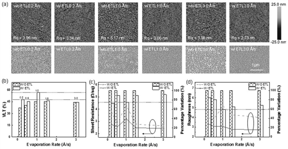
[0051]The transparent conductive glass etched with ITO on the entire surface is cleaned with lye, deionized water, acetone, isopropanol and ethanol in sequence, dried, and then treated with ultraviolet ozone for 5 minutes; then spin-coated on the surface of the conductive glass Concentration of 1mg / mL Bis-FIMG (about 8nm), and then directly on the Bis-FIMG film at different evaporation rates A 15nm thin layer of silver was evaporated.
[0052] The roughness was measured with an atomic force microscope, such as figure 1 As shown in a, the transmittance of the entire glass / ITO / Ag (15nm) electrode is measured with a u-v ultraviolet spectrophotometer, and the change of the transmittance value is as follows figure 1 As shown in b, the four-probe resistance meter measures its surface resistance, and the statistical value is as follows figure 1 as shown in c. Roughness variation values such as figure 1 d. It can be seen from the AFM images that the thin layer of silver evapor...
Embodiment 2
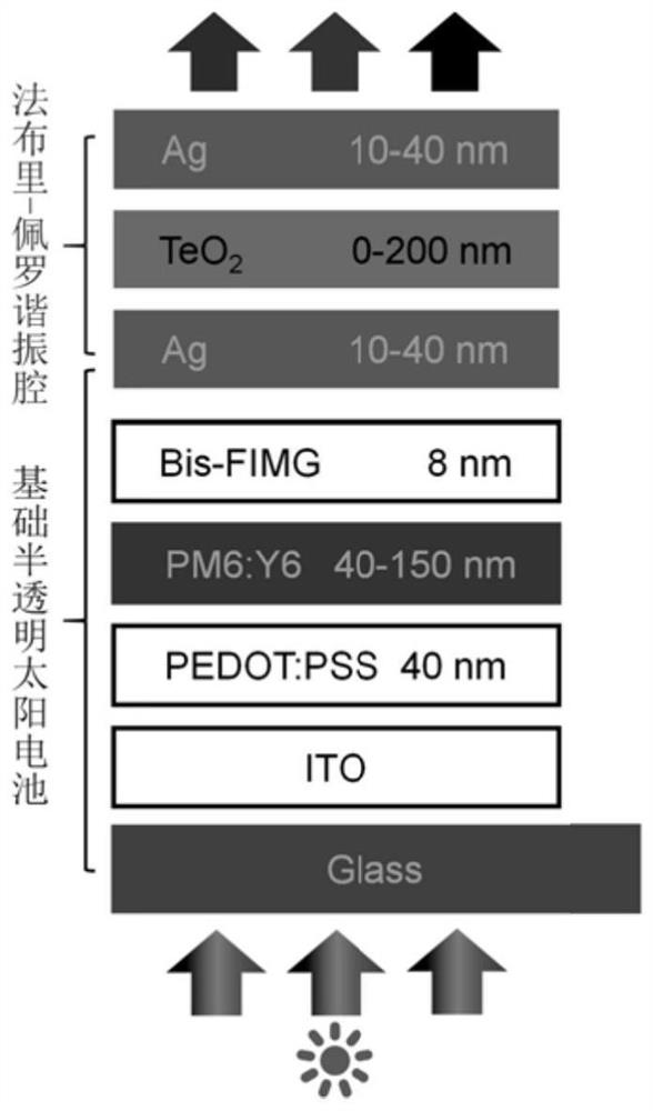
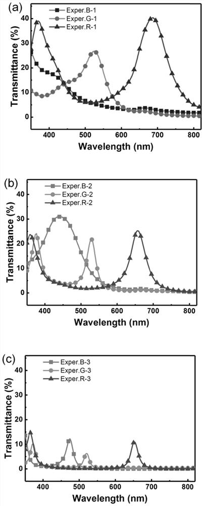
[0065] The transparent conductive glass with strip-shaped ITO (anode) etched on the surface is cleaned with lye, deionized water, acetone, isopropanol and ethanol by ultrasonic oscillation, dried, and then treated with ultraviolet ozone for 15 minutes; A layer of PEDOT:PSS was spin-coated on the surface at a rotation speed of 4600 rpm for 40 seconds, and then annealed at 140° C. for 20 minutes. Then the sheet was transferred to the glove box, and the PM6:Y6 mass ratio of 1:1.2, PM6, Y6 mixture of different concentrations was spin-coated for 30 seconds at different speeds to obtain active layers with different thicknesses, and then 1 mg / mL of Bis-FIMG solution was spin-coated on the active layer at a speed of 3500rpm to obtain a Bis-FIMG film with a thickness of about 8nm. Finally, with the vapor deposition apparatus to Evaporate thin-layer silver films with different thicknesses at the same speed, and then continue to evaporate TeO on the surface of thin-layer silver 2 and...
PUM
| Property | Measurement | Unit |
|---|---|---|
| thickness | aaaaa | aaaaa |
| thickness | aaaaa | aaaaa |
| thickness | aaaaa | aaaaa |
Abstract
Description
Claims
Application Information