Flexible implantable neural photoelectrode and preparation method thereof

An implantable photoelectrode technology, applied in the field of neuroscience, can solve the problems of limited device integration, difficulty in long-term in vivo recording, and great difference in Young's modulus, and achieve long-term in vivo stable recording and high-density signal recording , reduce the effect of nerve scarring

Pending Publication Date: 2020-11-17
SHANGHAI INST OF MICROSYSTEM & INFORMATION TECH CHINESE ACAD OF SCI
View PDF0 Cites 7 Cited by
  • Summary
  • Abstract
  • Description
  • Claims
  • Application Information

AI Technical Summary

Problems solved by technology

[0005] However, the power consumption of the LED chip implanted in the photoelectrode of the LED light source is relatively high, and the heating of the LED chip will cause damage to the brain tissue, and the size of the LED chip limits the improvement of the integration of the device, making it difficult to achieve multi-channel high-density recording; Waveguide implanted photoelectrodes are mostly processed on a hard silicon substrate. The Young’s modulus of the hard probe on the silicon substrate is very different from that of the brain tissue. Device implantation will cause brain tissue damage and nerve scars, which is difficult to achieve. Long-term in vivo recording, easy to cause damage to the experimental body

Method used


Image

  • Flexible implantable neural photoelectrode and preparation method thereof
  • Flexible implantable neural photoelectrode and preparation method thereof
  • Flexible implantable neural photoelectrode and preparation method thereof

Examples


Embodiment 1

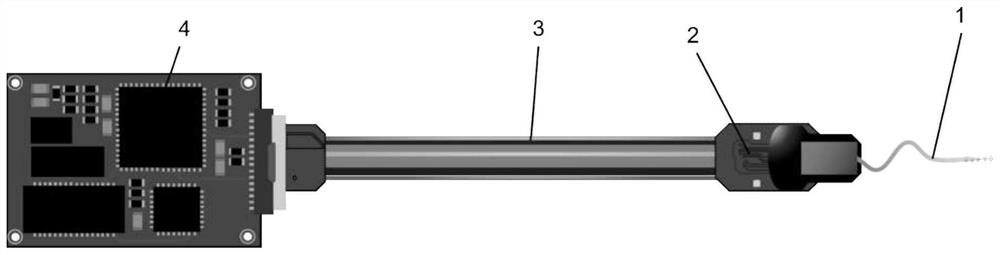
[0063] This embodiment provides a flexible implantable neural photoelectrode, and the flexible implantable neural photoelectrode 1 is arranged at the front end of a neuroimaging system with photoelectric stimulation and recording functions. The structure of the neuroimaging system is as follows figure 1 shown. The front end of the neuroimaging system is the flexible implantable neurophotoelectrode 1 , and the electrical and optical access points of the flexible implantable neurophotoelectrode 1 are drawn out through a small PCB circuit board 2 . The small PCB circuit board 2 is connected with the back-end EEG dedicated processing chip 4 of the neuroimaging system through a flexible cable 3 . Wherein, the flexible cable 3 includes an optical fiber and a cable. The back-end dedicated EEG processing chip 4 is used to collect the EEG signals obtained by the front-end of the neuroimaging system and further analyze and process the obtained EEG signals.

[0064] The structure of t...

Embodiment 2

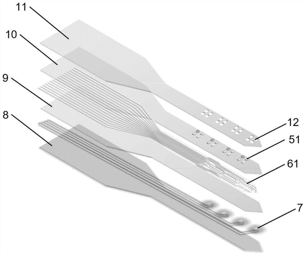
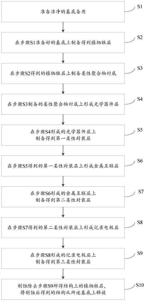
[0067] This embodiment provides a method for preparing the above-mentioned flexible implantable neural photoelectrode 1, see image 3 as well as figure 2 and Figure 4 , the method includes the following steps:

[0068] S1: Prepare a clean substrate 13 for use.

[0069] Preferably, the substrate 13 is a single-polished silicon wafer with a thickness of 300-500 μm (for example, 400 μm), and the single-polished silicon wafer is cleaned and ready for use.

[0070] S2: Prepare a nickel sacrificial layer 14 on the substrate 13 prepared in step S1.

[0071] Specifically, photoresist (such as SU-8 photoresist) is patterned by photolithography on the single-polished silicon wafer prepared in step S1, and a layer thickness is prepared on the photoresist by thermal evaporation deposition process. The metal nickel is 50-150 nm (for example, 100 nm), and the metal nickel is subjected to a lift-off process to obtain the nickel sacrificial layer 14 .

[0072] S3: Prepare a flexible po...

Embodiment 3

[0091]This embodiment provides a method for implanting the above-mentioned flexible implantable neural photoelectrode 1 into the mouse brain for optogenetics research. The specific implantation method of the flexible implantable neural photoelectrode 1 is as follows:

[0092] 1) First, weld the structure obtained in the second embodiment through step S9 to the PCB circuit board 2 at the rear end of the neuroimaging system, and then align the optical fiber 15 to the input grating 721 at a certain angle through the bracket 16 and fix it on the PCB circuit board 2 Above, the incident light will be emitted from the optical fiber 15 and coupled into the tapered waveguide 711 through the input grating 721. The tapered waveguide 711 converts the optical transmission mode from multi-mode to single-mode, and enters the subsequent single-mode waveguide 71 for transmission, such as Figure 5 shown;

[0093] 2) Etching and removing the nickel sacrificial layer on the structure obtained i...


PUM


Abstract

The invention discloses a flexible implantable neural photoelectrode. The flexible implantable neural photoelectrode comprises a recording electrode layer, a metal interconnection layer and an opticaldevice layer which are sequentially arranged, wherein a plurality of electrode sites are arranged on the recording electrode layer, the metal interconnection layer is used for connecting the electrode sites with the rear end of a neural imaging system, and the optical device layer is used for transmitting laser from the rear end of the neural imaging system to the flexible implantable neural photoelectrode and emitting the laser. The invention further discloses a method for preparing the flexible implantable neural photoelectrode. The flexible implantable neural photoelectrode provided by theinvention is high in integration level, and multi-channel and high-density signal recording can be realized; the size of the part implanted into the brain is small, so that the damage of device implantation to the brain tissue can be reduced; a flexible material is adopted to be matched with the Young modulus of the brain tissue, so that the nerve scar caused in the in-vivo device implantation process can be reduced, and long-term in-vivo stable recording is realized; and accurate stimulation, in-situ recording and cross-brain-region synchronous recording can be realized through photoelectricsignal interconnection.

Description

technical field [0001] The invention relates to the technical field of neuroscience, in particular to a flexible implantable neural photoelectrode and a preparation method thereof. Background technique [0002] The photoelectrode is an electrophysiological device that integrates the functions of light stimulation and electrical activity recording, and is mainly used in conjunction with optogenetics technology. At present, people usually use the combination of optical technology and genetic technology to achieve selective control of cell behavior, and design and prepare devices that can simultaneously realize light regulation and multi-channel electrophysiological recording, that is, neural photoelectrodes. [0003] The simplest neural photoelectrode is the optical fiber electroplating photoelectrode, which electroplates a metal layer on the tapered fiber head, and then encapsulates the metal layer with an insulating layer to only expose the electrical recording point at the ...

Claims


Application Information

Patent Timeline
Patent Type & Authority Applications(China)
IPC IPC(8): A61B5/04
Inventor 陶虎顾驰周志涛魏晓玲杨会然
Owner SHANGHAI INST OF MICROSYSTEM & INFORMATION TECH CHINESE ACAD OF SCI
Why Eureka
Try Eureka