Post-cutting passivation method of silicon-based semiconductor device and silicon-based semiconductor device

A semiconductor and post-passivation technology, which is applied in the field of silicon-based semiconductor devices and post-cutting passivation of silicon-based semiconductor devices, can solve the problems of battery sheet efficiency drop and conversion efficiency drop

Active Publication Date: 2020-11-17
JINKO GREEN ENERGY SHANGHAI MANAGEMENT CO LTD +1
View PDF16 Cites 9 Cited by
  • Summary
  • Abstract
  • Description
  • Claims
  • Application Information

AI Technical Summary

Problems solved by technology

However, the conversion efficiency of small cells treated by this cutting method has decreased.
[0004] Therefore, how to provide a cutting method that can effectively solve the problem of the decrease in cell efficiency caused by cutting has become a technical problem to be solved urgently by those skilled in the art

Method used


Image

  • Post-cutting passivation method of silicon-based semiconductor device and silicon-based semiconductor device
  • Post-cutting passivation method of silicon-based semiconductor device and silicon-based semiconductor device
  • Post-cutting passivation method of silicon-based semiconductor device and silicon-based semiconductor device

Examples


Embodiment 1

[0134] The first passivation layer is a silicon oxide layer, which can be made by oxidation reaction. Since hot oxygen requires high temperature, it can be combined with surface smoothing treatment steps, the specific steps are as follows.

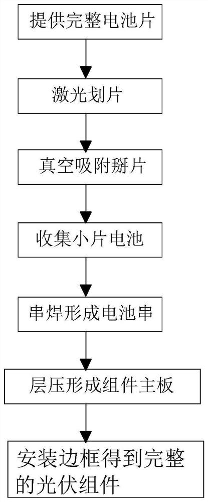
[0135] (1) The complete silicon-based semiconductor device is divided to obtain small silicon-based semiconductor devices.

[0136] (2) Place a small silicon-based semiconductor device in a low-pressure vacuum environment, and use a high-energy particle beam, such as He ions, to bombard the cross-section through an accelerator and focus. At this time, the temperature of the cavity where the silicon-based semiconductor device is located should not exceed 350°C.

[0137] (3) After the high-energy particle beam bombardment, nitrogen, water vapor and oxygen can be sprayed on the section. At this time, the temperature of the silicon-based semiconductor device is 150°C-250°C, and the gaseous water vapor and oxygen react with the silicon surfac...

Embodiment 2

[0141] The first passivation layer is a silicon oxide layer, which can be obtained by an ozone oxidation method, and the specific steps are as follows.

[0142] (1) The complete silicon-based semiconductor device is divided to obtain small silicon-based semiconductor devices.

[0143] (2) Place a small silicon-based semiconductor device in a low-pressure vacuum environment, and use a high-energy particle beam, such as He ions, to bombard the cross-section through an accelerator and focus. At this time, the temperature of the cavity where the silicon-based semiconductor device is located should not exceed 350°C.

[0144] (3) After the high-energy particle beam bombardment, ozone can be sprayed on the cross section. At this time, the silicon-based semiconductor device is still in the low-pressure vacuum chamber, and is not taken out to be in contact with the air, so as to avoid the oxygen in the air from causing a natural oxide layer of extremely poor quality on the silicon-bas...

Embodiment 3

[0148] The first passivation layer is a silicon nitride layer, which can be obtained by chemical deposition, and the specific steps are as follows.

[0149] (1) The complete silicon-based semiconductor device is divided to obtain small silicon-based semiconductor devices.

[0150] (2) Place a small piece of silicon-based semiconductor device in a low-pressure vacuum environment, and use a high-energy particle beam, such as He ions or Ne ions, to bombard the cross-section through an accelerator and focus. At this time, the temperature of the cavity where the silicon-based semiconductor device is located should not exceed 350°C.

[0151] (3) After the bombardment of the high-energy particle beam is completed, the method of chemical vapor deposition is used to pass the plasma mixed with ammonia gas and silane to the cross-sectional surface to complete the silicon nitride film deposition process. The thickness of the film layer can be set by the reaction time. Preferably, the thi...


PUM

PropertyMeasurementUnit
thicknessaaaaaaaaaa
thicknessaaaaaaaaaa
thicknessaaaaaaaaaa

Abstract

The invention provides a post-cutting passivation method of a silicon-based semiconductor device and the silicon-based semiconductor device, and relates to the technical field of semiconductor devices. The post-cutting passivation method of the silicon-based semiconductor device comprises the following steps: cutting a preset area of the silicon-based semiconductor device by using a cutting process to form a first surface related to the preset area; smoothing the first surface to adjust the surface morphology of the first surface, so that the height difference between bulges and recesses in anon-edge region on the first surface is less than 20nm; and the smoothed first surface is passivated so as to form a first passivation layer on the first surface. According to the invention, the problem of efficiency reduction caused by cutting of the silicon-based semiconductor device can be reduced or avoided, and the silicon-based semiconductor device with higher efficiency can be obtained.

Description

technical field [0001] The present application relates to the technical field of semiconductor devices, in particular to a post-cut passivation method for silicon-based semiconductor devices and the silicon-based semiconductor device. Background technique [0002] A solar cell is a semiconductor device with energy conversion function based on semiconductor materials, and is the core device of solar photovoltaic power generation. Solar cells include silicon-based solar cells, which belong to silicon-based semiconductor devices. In recent years, photovoltaic power generation technology, as a mainstream technology for utilizing solar energy resources, is an important field for the development of green energy, and has moved towards marketization and commercialization. With the continuous advancement of technology, the development trend of photovoltaic module products is the continuous improvement of output power. The research focus of related photovoltaic module companies is to...

Claims


Application Information

Patent Timeline
Patent Type & Authority Applications(China)
IPC IPC(8): H01L31/18H01L31/0352H01L31/0216H01L31/068
CPCH01L31/186H01L31/1868H01L31/035281H01L31/02167H01L31/0682Y02E10/547H01L31/1804Y02P70/50
Inventor 袁雪婷张昕宇
Owner JINKO GREEN ENERGY SHANGHAI MANAGEMENT CO LTD
Why Eureka
Try Eureka