All-solid-state chip large-angle optical beam forming system

A beamforming and chip-based technology, applied in the field of all-solid-state chip-based large-angle optical beamforming systems, can solve the problems of limited wavelength range of laser tuning, affecting the application performance of OPA technology, and limited beam scanning angle, etc., to achieve small hardware complexity The effect of sacrificing degree, improving integrability, and simplifying hardware complexity

Active Publication Date: 2020-12-04
AEROSPACE INFORMATION RES INST CAS
View PDF5 Cites 9 Cited by
  • Summary
  • Abstract
  • Description
  • Claims
  • Application Information

AI Technical Summary

Problems solved by technology

On the one hand, commercial large-scale tunable light sources mostly use the principle of external cavity, relying on the adjustment of mechanical structure, large volume, slow speed, and difficult to integrate; on the other hand, limited by the gain bandwidth of semiconductor materials, the tuning wavelength range of lasers is limited, so relatively Compared with the phased array dimension, the wavelength dimension has the problem of limited beam scanning angle, which will affect the application performance based on OPA technology, such as limiting the imaging range of lidar and the coverage of space optical communication, so it is necessary to expand the beam scanning range of the system

Method used


Image

  • All-solid-state chip large-angle optical beam forming system
  • All-solid-state chip large-angle optical beam forming system
  • All-solid-state chip large-angle optical beam forming system

Examples


Embodiment Construction

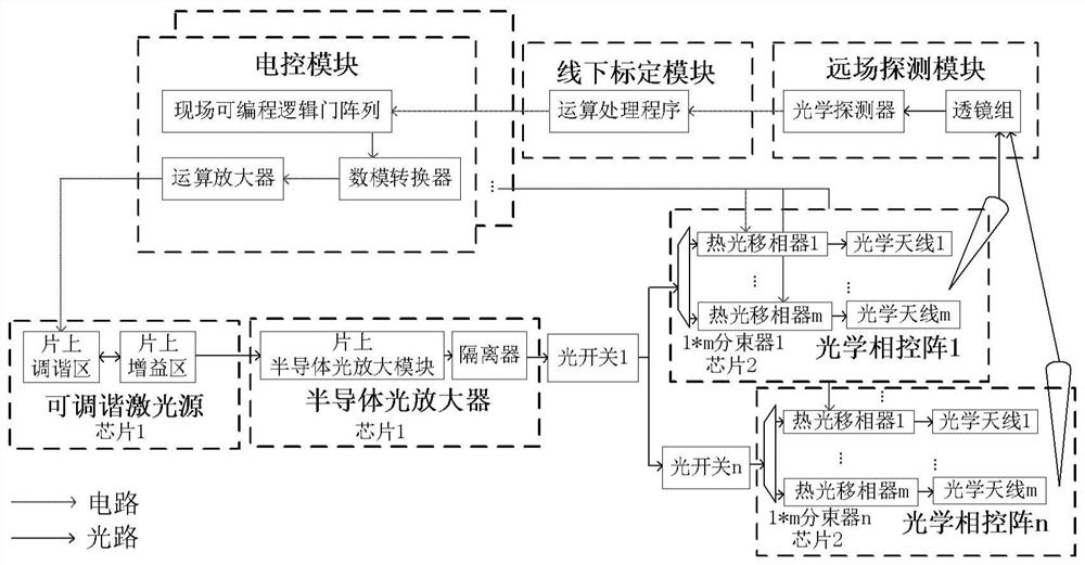
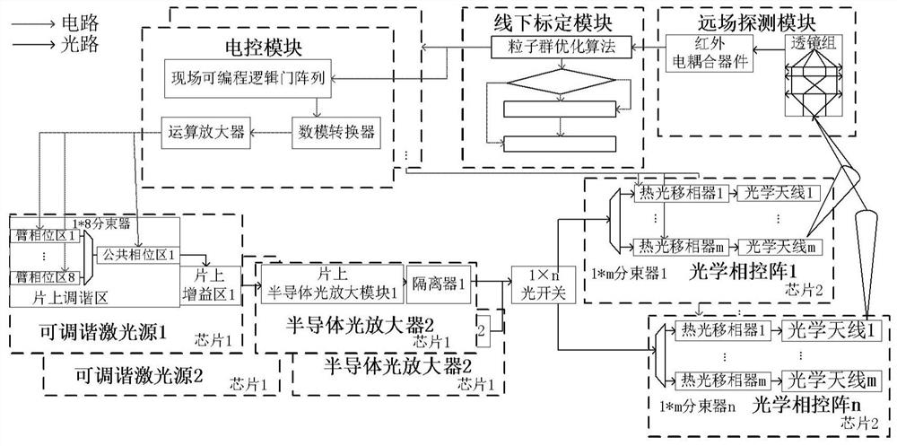
[0048] like figure 1 As shown, it is a schematic structural diagram of an all-solid-state chip-based large-angle optical beamforming system of the present invention, including:

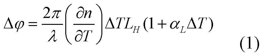
[0049] A tunable laser source that will be above the source threshold I th The pumping current of the laser is injected into the gain region of the laser, and the single-mode laser with a wavelength of λ is independently emitted by the light source, and is transmitted from the front end of the laser to the semiconductor optical amplifier through the on-chip waveguide; the laser needs to be single-mode, that is, single longitudinal mode + single transverse mode The reasonable design of the waveguide cross section can easily ensure the single transverse mode; the control of the single longitudinal mode of the device is often more complicated.

[0050] Semiconductor optical amplifier, by injecting appropriate driving current, amplifies the laser power from the tunable laser source to a high enough level...


PUM


Abstract

An all-solid-state chip optical beam forming system comprises a tunable light source, a semiconductor optical amplifier, an optical phased array, a far-field detection module, an offline calibration module and an electric control module, wherein the semiconductor optical amplifier amplifies the laser power from the tunable light source by injecting a proper driving current, and transmits the laserpower to the optical phased array through the on-chip waveguide; or the semiconductor optical amplifier and the tunable light source are integrated together and transmitted to the optical phased array through the coupling optical fiber; according to the optical phased array, single longitudinal mode laser enters from a cleavage surface and is equally divided into m paths of waveguides by a properamount of optical beam splitters, and the laser in each waveguide is equal in power; after passing through the thermal regulation electrodes loaded on the waveguides, the waveguides are arranged at certain intervals and radiated into a free space above the waveguides through gratings etched at the tail ends of the waveguides, and m paths of array element radiation beams are superposed to form a phased-array antenna directional diagram of a phase dimension; and the radiation direction of the grating at the tail end of the optical phased array waveguide is changed by tuning the wavelength of the light source.

Description

technical field [0001] The invention relates to the technical field of beam scanning and control, in particular to an all-solid-state chip large-angle optical beam forming system. Background technique [0002] Beam scanning and control technology plays a central role in cutting-edge optical applications such as lidar and space optical communication. Compared with radio frequency beams, beams have the advantages of good directivity and high resolution, and can support high-precision, all-day, high imaging resolution lidar detection, serving the fields of automatic driving, environmental monitoring, military reconnaissance, etc., fast and accurate perceive the surrounding environment. In addition, the divergence angle of the beam is small, the possibility of being intercepted and eavesdropped is low, the link is safer, and the carrier frequency is higher. It can support space optical communication and serve the access and transmission of B5G / 6G high-speed information. [000...

Claims


Application Information

Patent Timeline
Patent Type & Authority Applications(China)
IPC IPC(8): G02F1/29
CPCG02F1/292
Inventor 李王哲马尉超刘宸钰
Owner AEROSPACE INFORMATION RES INST CAS
Why Eureka
Try Eureka