Manufacturing method and structure of miniaturized three-dimensional inductor with magnetic core

A manufacturing method and inductance technology, which can be used in magnetic core manufacturing, inductance/transformer/magnet manufacturing, transformer/inductor magnetic core, etc., can solve the problems of increasing magnetic core eddy current loss, restricting industrialization development, and restricting inductance performance, etc. Achieve the effect of small scattered magnetic flux, increase inductance capacity and performance optimization space, and high magnetic induction intensity

Active Publication Date: 2020-12-15
UNIV OF ELECTRONICS SCI & TECH OF CHINA +1
View PDF6 Cites 0 Cited by
  • Summary
  • Abstract
  • Description
  • Claims
  • Application Information

AI Technical Summary

Problems solved by technology

However, the ferrite layer formed by screen printing should be sintered at a temperature of 900-1000°C, which is incompatible with the standard integrated circuit manufacturing process; the thickness of the magnetic core produced by the sputtering process is limited and the cost is high , which limits the industrial development of this technology; the inductance Q value of the magnetic material core using electroplating film formation is generally lower than the Q value of film formation materials using sputtering technology or screen printing technology, the main reason is the magnetic material. Due to the conductivity, when the operating frequency of the inductor increases, the eddy current loss of the core will increase
In addition to the compatibility of magnetic materials and microelectronics processes, semiconductor processes are generally planar processes, which can only realize chip inductors, which greatly limits the performance of inductors

Method used


Image

  • Manufacturing method and structure of miniaturized three-dimensional inductor with magnetic core
  • Manufacturing method and structure of miniaturized three-dimensional inductor with magnetic core
  • Manufacturing method and structure of miniaturized three-dimensional inductor with magnetic core

Examples


Embodiment Construction

[0038] The present invention will be further described below through specific embodiments.

[0039] refer to Figure 1 to Figure 13 , a method for manufacturing a miniaturized three-dimensional inductor with a magnetic core, comprising the steps of:

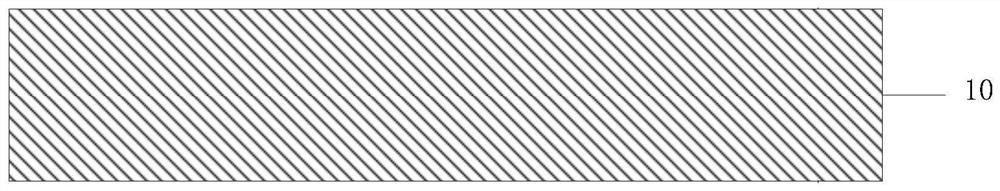
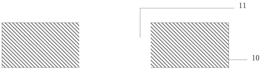
[0040] 1) Fabricate at least one microgroove structure 11 on the magnetic substrate 10 . The magnetic substrate is sheet-shaped, has a front side and a back side, is made of magnetic material, is square or circular in shape, and has a thickness of 0.05-3mm.

[0041] The manufacturing process of the micro-groove structure 11 may be laser etching, plasma bombardment, sandblasting or ultrasonic etching, etc., and the side length of the micro-groove structure 11, that is, the width or length, is 0.05-3 mm. The number and shape of the micro-groove structures 11 are not limited. In the magnetic substrate, the magnetic core is formed outside the micro-groove structure, that is, the magnetic core surrounds the micro-groove junction. ...


PUM

PropertyMeasurementUnit
thicknessaaaaaaaaaa

Abstract

The invention discloses a manufacturing method and structure of a miniaturized three-dimensional inductor with a magnetic core. The manufacturing method comprises the following steps of 1) manufacturing at least one microgroove structure on a magnetic substrate; 2) manufacturing a plurality of through holes in the hidden frame substrate, and filling metal materials in the through holes; 3) cuttingthe hidden frame substrate to form a plurality of hidden frames with metal materials, and embedding and fixing the hidden frames into the microgroove structures; and 4) respectively manufacturing a first plane interconnection structure and a second plane interconnection structure on the front surface and the back surface of the magnetic substrate, wherein the first plane interconnection structureand the second plane interconnection structure are respectively and electrically connected with the metal material of the hidden frame to form at least one inductance winding. The present invention achieves a high-capacity miniaturized inductor device.

Description

technical field [0001] The invention relates to the fields of magnetic material processing, microelectronic technology and magnetic components, in particular to a manufacturing method and structure of a three-dimensional inductor. Background technique [0002] With the improvement of the performance of electronic products, the level of miniaturization, light weight and integration of electronic products is getting higher and higher, the operating frequency of the system is continuously increasing, the operating voltage is getting lower and lower, and the quality requirements of the system for signal transmission are also increasing. High, traditional solutions have been unable to fully meet the technical requirements of new technologies for high-density system integration; at the same time, the miniaturization and integration of passive components have also become an important bottleneck restricting the development of electronic systems. In order to solve this problem, resea...

Claims


Application Information

Patent Timeline
Patent Type & Authority Applications(China)
IPC IPC(8): H01F41/04H01F41/02H01F27/28H01F27/24
CPCH01F41/04H01F41/0206H01F27/28H01F27/24
Inventor 薛恺钟智勇郑宗森叶根祥林志滨王康
Owner UNIV OF ELECTRONICS SCI & TECH OF CHINA
Why Eureka
Try Eureka