Semiconductor light-emitting unit and cascaded mid-infrared light-emitting diode
A technology of light-emitting diodes and light-emitting units, which is applied in the direction of semiconductor devices, electrical components, and electric solid-state devices, and can solve the problems of poor repeatability and uniformity in the growth process, affecting quantum efficiency and output power, and escaping carriers to be recombined. Achieve the effects of suppressing non-radiative recombination, improving quantum efficiency and output power, and increasing device voltage
- Summary
- Abstract
- Description
- Claims
- Application Information
AI Technical Summary
Problems solved by technology
Method used
Image

Examples
Embodiment 1
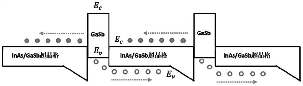
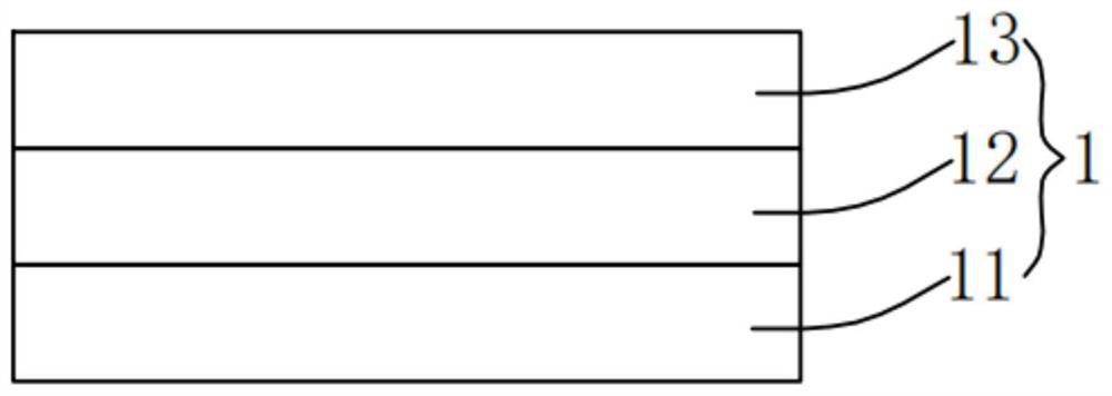
[0026] This embodiment provides a semiconductor light emitting unit 1, such as figure 2 As shown, the semiconductor light emitting unit 1 includes a hole barrier layer 11 , an active layer 12 and an electron barrier layer 13 which are sequentially stacked. Such as Figure 4 As shown, in order to respectively set heterojunction structures on both sides of the active layer 12, in this embodiment, the hole barrier layer 11 and the electron barrier layer 13 of the semiconductor light emitting unit 1 The effective bandwidth is respectively greater than the effective bandwidth of the active layer 12 .
[0027] Wherein, the conduction bands of the hole barrier layer 11 and the active layer 12 are flush with each other and the valence bands form a potential difference, thereby limiting the mobility of hole carriers; the electron barrier layer 13 The valence bands of the active layer 12 are flush with each other and the conduction band forms a potential difference, thereby limiting ...
Embodiment 2
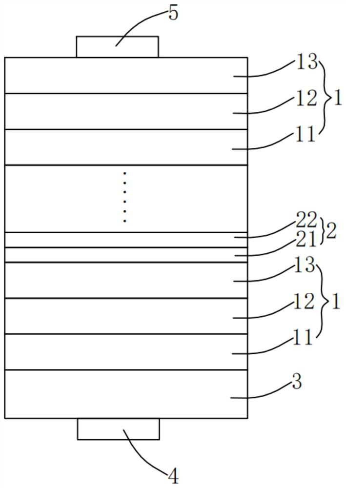
[0031] This embodiment provides a cascaded mid-infrared light emitting diode, such as image 3 As shown, the cascaded mid-infrared light-emitting diode includes a substrate 3, and a plurality of stacked semiconductor light-emitting units 1 as described in Embodiment 1 are arranged on the first surface of the substrate 3, and each of the The electron barrier layer 13 of the semiconductor light emitting unit 1 faces the hole barrier layer 11 of the adjacent semiconductor light emitting unit 1, wherein a tunnel junction is provided between every two adjacent semiconductor light emitting units 1 2. A first electrode 4 is provided on the second surface of the substrate 3, and a second electrode 5 corresponding to the first electrode 4 is provided on the light emitting unit that is farthest from the substrate 3.
[0032] Wherein, the tunnel junction 2 includes a stacked P-type GaSb layer 21 and an N-type InAs layer 22 . The P-type GaSb layer 21 faces the electron barrier layer 13 ...
Embodiment 3
[0036] This embodiment discloses a method for manufacturing the cascaded mid-infrared light-emitting diode of Embodiment 2, the method comprising:
[0037] Step S1 , growing the semiconductor light emitting unit 1 and the tunnel junction 2 alternately on the first surface of the substrate 3 , and finishing the growth operation after setting the 15th semiconductor light emitting unit 1 . Specifically, the substrate 3 is preferably an N-type InAs substrate with a doping concentration of 1×10 19 cm -3. Metal-organic chemical vapor deposition (MOCVD) is used as the growth process, the growth source is TMIn, TMGa, TMSb, AsH3 and PH3, the N-type dopant source is SiH4, the P-type dopant source is DEZn, the growth temperature is 600°C, and the reaction chamber pressure It is 200Torr. After the impurities on the surface of the substrate 3 are removed by high temperature treatment, the following growths are performed in sequence:
[0038] The hole barrier layer 11 includes a 100nm t...
PUM
 Abstract
Description
Claims
Application Information
 - R&D
- Intellectual Property
- Life Sciences
- Materials
- Tech Scout
- Unparalleled Data Quality
- Higher Quality Content
- 60% Fewer Hallucinations
Browse by: Latest US Patents, China's latest patents, Technical Efficacy Thesaurus, Application Domain, Technology Topic, Popular Technical Reports.
© 2025 PatSnap. All rights reserved.Legal|Privacy policy|Modern Slavery Act Transparency Statement|Sitemap|About US| Contact US: help@patsnap.com